Display device and electronic device including display device

a technology of electronic devices and display devices, which is applied in the field of display devices and electronic devices, can solve the problems of increasing power consumption of display devices and pixel aperture ratios, and achieve the effects of suppressing the driving voltage of light-emitting elements, increasing aperture ratios, and increasing aperture ratios

Active Publication Date: 2011-04-21
SEMICON ENERGY LAB CO LTD
View PDF101 Cites 64 Cited by
  • Summary
  • Abstract
  • Description
  • Claims
  • Application Information

AI Technical Summary

Benefits of technology

[0016]Further, a decrease in energy supplied to a light-emitting element included in a self-luminous display device or a transmissive display device for reducing power consumption of the display device has a significant influence on the display quality such as dark display or display disappearance.
[0017]Further, the reflective display devices in each of which a light-storing material is used, which are disclosed in the above patent documents, can perform display with low power consumption even in an environment where the amount of external light is small; however, the light-storing material needs to be irradiated with external light in advance in order to store the light. Therefore, such a reflective display device is not suitable for long-term use in a dark place.
[0023]Further, one embodiment of the present invention focuses on power consumed by a driver circuit included in a self-luminous display device. In other words, power consumed by the display device may be reduced by decreasing the frequency of operation of the driver circuit. In addition, power consumed by the display device may be reduced in such a manner that a light-storing layer is provided in a pixel portion of the self-luminous display device, light emitted from a light-emitting element is stored in the light-storing layer, and energy supplied to the light-emitting element is suppressed while an image is displayed with the use of light emitted from the light-storing layer.
[0036]According to one embodiment of the present invention, a circuit is formed using a thin film transistor in which a highly-purified oxide semiconductor is used, whereby operation of the circuit included in a display device can be stabilized. In addition, off-state current reduced to 1×10⁻¹³ A or lower allows omission of a capacitor which holds signal voltage applied to a pixel of the display device. In other words, a storage capacitor does not need to be provided in each pixel, which results in an increase in aperture ratio. When aperture ratio is increased, driving voltage of a light-emitting element is suppressed, which results in a reduction in power consumption of the display device.
[0037]Further, a pixel which is formed using the thin film transistor according to one embodiment of the present invention can maintain a constant state (a state in which an image signal is written), and thus can operate stably even in the case where a still image is displayed. In addition, operation interval of a driver circuit can be extended, which results in a reduction in power consumption of a display device.
[0038]Further, according to one embodiment of the present invention, a display device that can be used in an environment where external light is weak can be provided. In addition, a display device that can display an image with power consumption suppressed can be provided.

Problems solved by technology

The provision of the capacitor in the pixel causes problems such as a decrease in aperture ratio of the pixel and an increase in power consumption of the display device.

Method used


Image

  • Display device and electronic device including display device
  • Display device and electronic device including display device
  • Display device and electronic device including display device

Examples


embodiment 1

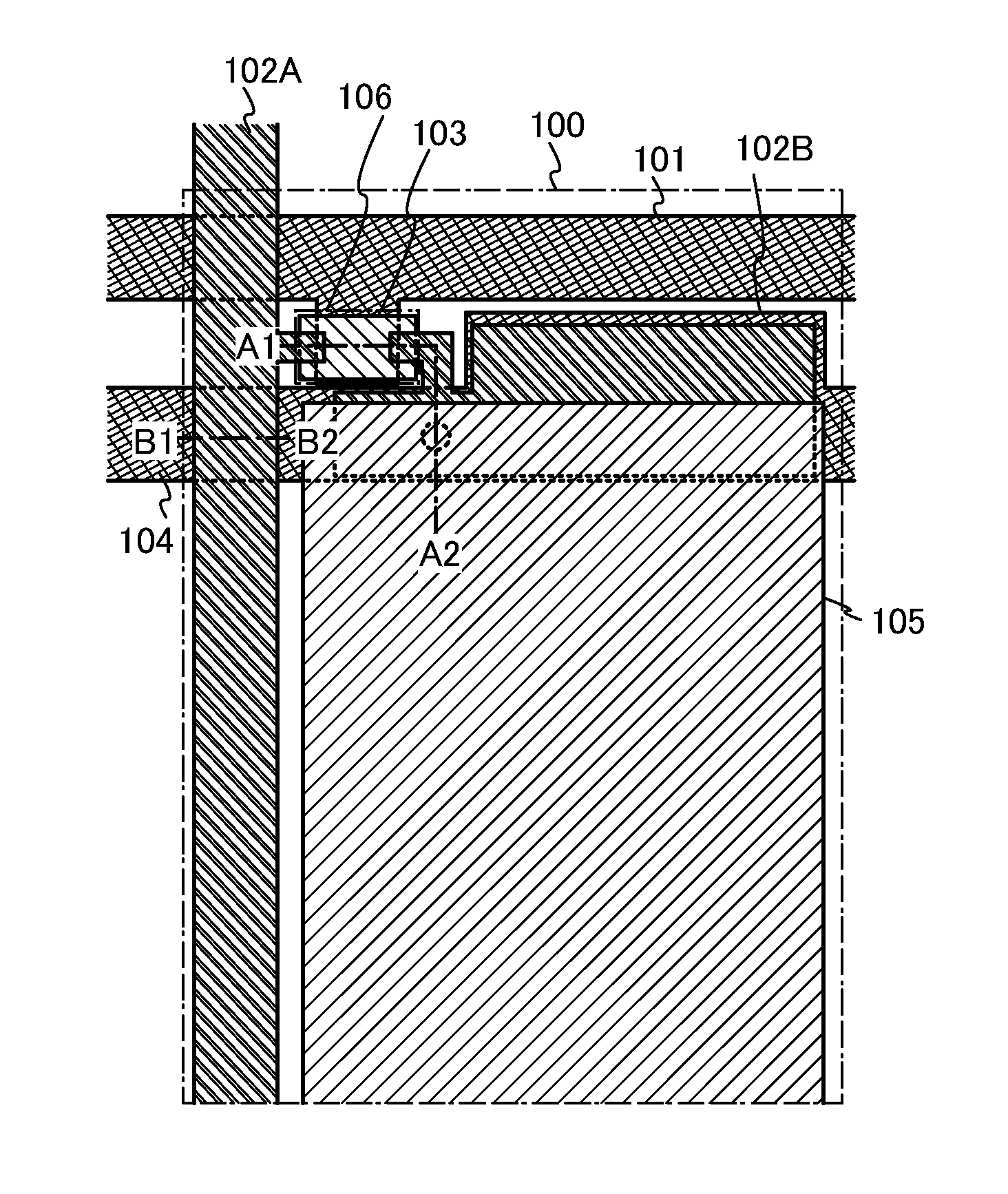
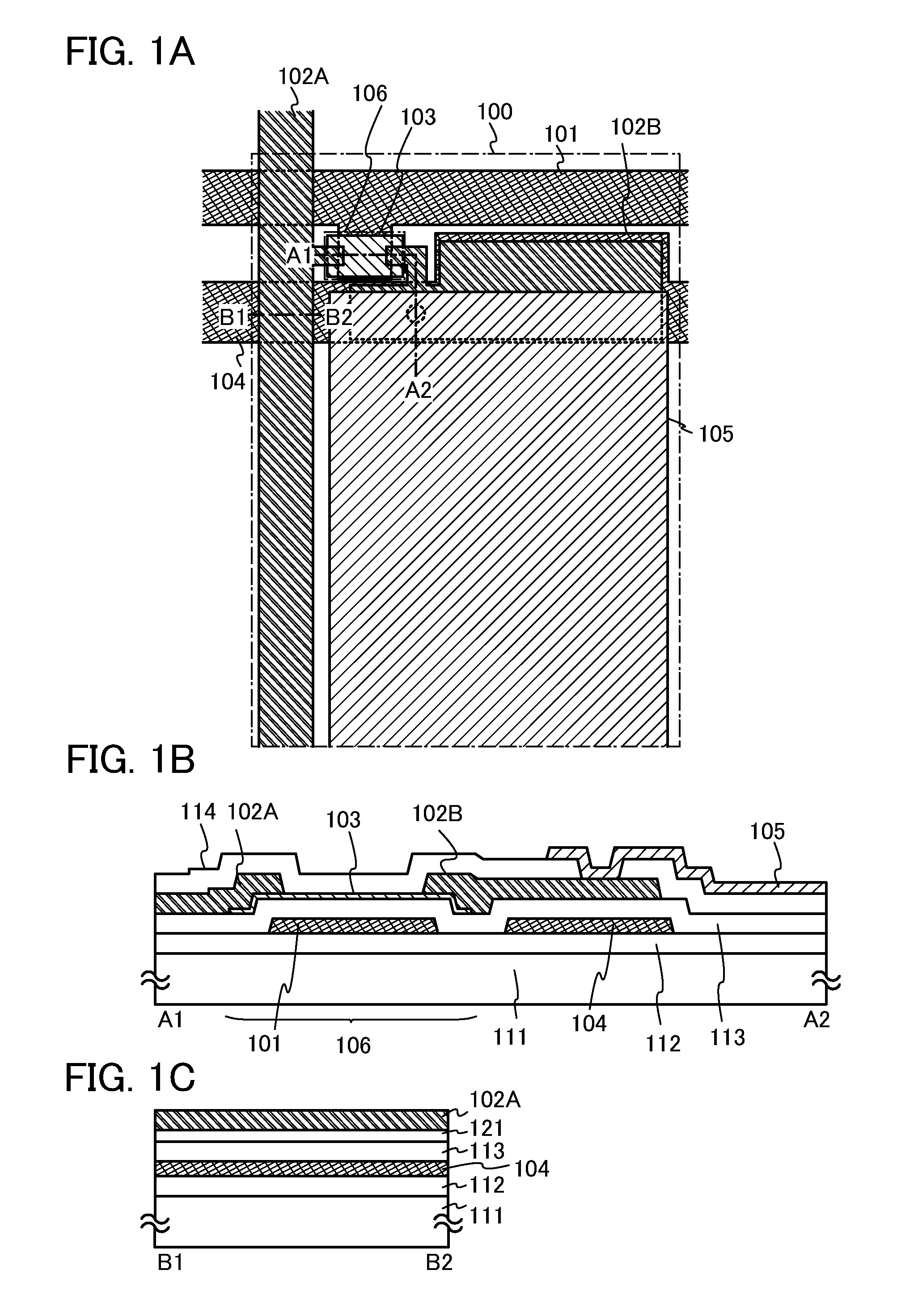
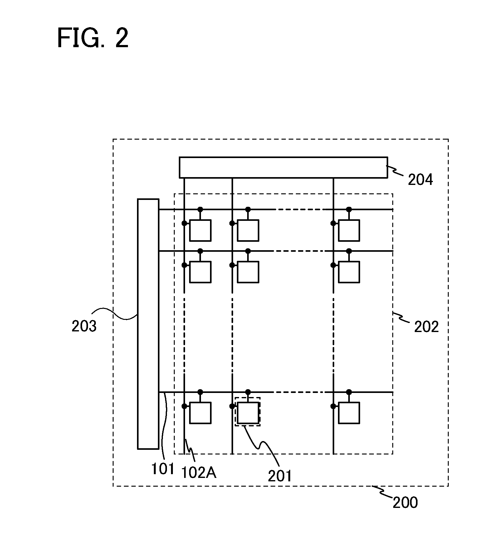
[0070]In this embodiment, an example of a pixel including a thin film transistor in which a highly-purified oxide semiconductor is used and a pixel electrode will be described below with reference to FIGS. 1A to 1C, FIG. 2, FIG. 3, and FIGS. 4A and 4B.

[0071]First, FIG. 1A is a top view of the pixel. Note that as an example of a structure of a TFT illustrated in FIG. 1A, a bottom gate structure that is a so-called inverted staggered structure is illustrated, in which wiring layers that serve as source and drain electrodes of a TFT are provided on one side of an oxide semiconductor layer that serves as a channel region, and a wiring that serves as a gate is provided on the other side of the oxide semiconductor layer. A pixel 100 illustrated in FIG. 1A includes a first wiring 101 that functions as a scan line, a second wiring 102A that functions as a signal line, an oxide semiconductor layer 103, a capacitor line 104, and a pixel electrode 105, and in addition to the above, a third wir...

embodiment 2

[0120]In this embodiment, an example of a thin film transistor that can be applied to the display device disclosed in this specification will be described. A thin film transistor 410 described in this embodiment can be used as the thin film transistor 106 in Embodiment 1.

[0121]An embodiment of a thin film transistor of this embodiment and an embodiment of a method for manufacturing the thin film transistor will be described with reference to FIGS. 5A and 5B and FIGS. 6A to 6E.

[0122]FIG. 5A illustrates an example of a top surface structure of a thin film transistor and FIG. 5B illustrates an example of a cross-sectional structure thereof. The thin film transistor 410 illustrated in FIGS. 5A and 5B is a top-gate thin film transistor.

[0123]FIG. 5A is a top view of the top-gate thin film transistor 410 and FIG. 5B is a cross-sectional view taken along line C1-C2 in FIG. 5A.

[0124]The thin film transistor 410 includes, over a substrate 400 having an insulating surface, an insulating layer...

embodiment 3

[0204]In this embodiment, an example of a thin film transistor that can be applied to the display device disclosed in this specification will be described. Note that for portions that are the same as those in Embodiment 2 and portions and steps that are similar to those in Embodiment 2, Embodiment 2 can be referred to, and description thereof is not repeated. In addition, detailed description of the same parts is omitted. A thin film transistor 460 described in this embodiment can be used as the thin film transistor 106 in Embodiment 1.

[0205]An embodiment of a thin film transistor of this embodiment and an embodiment of a method for manufacturing the thin film transistor will be described with reference to FIGS. 7A and 7B and FIGS. 8A to 8E.

[0206]FIG. 7A illustrates an example of a top surface structure of a thin film transistor and FIG. 7B illustrates an example of a cross-sectional structure thereof. The thin film transistor 460 illustrated in FIGS. 7A and 7B is a top-gate thin fi...


PUM


Abstract

Objects are to provide a display device the power consumption of which is reduced, to provide a self-luminous display device the power consumption of which is reduced and which is capable of long-term use in a dark place. A circuit is formed using a thin film transistor in which a highly-purified oxide semiconductor is used and a pixel can keep a certain state (a state in which a video signal has been written). As a result, even in the case of displaying a still image, stable operation is easily performed. In addition, an operation interval of a driver circuit can be extended, which results in a reduction in power consumption of a display device. Moreover, a light-storing material is used in a pixel portion of a self-luminous display device to store light, whereby the display device can be used in a dark place for a long time.

Description

TECHNICAL FIELD[0001]The present invention relates to display devices and electronic devices each including the display device. In particular, one embodiment of the present invention relates to a display device including a field effect transistor in which an oxide semiconductor is used and a light-emitting element, and an electronic device including the display device.BACKGROUND ART[0002]A technique for forming a thin film transistor (TFT) by using a semiconductor thin film formed over a substrate having an insulating surface has attracted attention. The thin film transistor has been used in a display device typified by a liquid crystal television. A silicon-based semiconductor material is known as a material of a semiconductor thin film that can be used in a thin film transistor. Besides, an oxide semiconductor has attracted attention as another material.[0003]As a material of the oxide semiconductor, zinc oxide or a substance containing zinc oxide is known. Thin film transistors e...

Claims


Application Information

Patent Timeline
Patent Type & Authority Applications(United States)
IPC IPC(8): G06F3/038
CPCG09G3/3233H01L27/1225G09G3/2003G09G3/3208H01L29/78609H01L29/7869H01L29/78693H01L29/78696G09G2330/021H10K59/1213H10K59/131H10K59/123G09G3/30
Inventor YAMAZAKI, SHUNPEIKOYAMA, JUNMIYAKE, HIROYUKI
Owner SEMICON ENERGY LAB CO LTD
Why Eureka
Try Eureka