Semiconductor device and method for manufacturing the same

a technology of semiconductor integrated circuits and integrated circuits, which is applied in the direction of semiconductor devices, diodes, electrical devices, etc., can solve the problems of not being mature or compatible with cmos currently, hardly being applied to the device requiring a higher driving capability, and facing a relative low device drive capability, etc., to achieve high performance and low power consumption , the effect of effective enhancement of the on-state current of

Active Publication Date: 2014-02-20
INST OF MICROELECTRONICS CHINESE ACAD OF SCI
View PDF6 Cites 378 Cited by
  • Summary
  • Abstract
  • Description
  • Claims
  • Application Information

AI Technical Summary

Benefits of technology

[0029]In accordance with the semiconductor device and method for manufacturing the same of the present invention, a GeSn alloy having a narrow band gap is formed by implanting precursors and then performing a laser rapid annealing, so that the on-state current of TFET is effectively enhanced, accordingly it has an important application prospect in a high performance low power consumption application.

Problems solved by technology

However, at the same time, the device drive capability is limited by the traditional technology of silicon material, the carrier mobility is low, thus a problem of a relatively low device drive capability is confronted with.
However, the lattice constants of the two materials are not sufficiently different from that of Si, they can only provide a limited strain, thus can hardly be applied to the device requiring a higher driving capability.
However, it need molecular-beam epitaxy or CVD to form the traditional GeSn alloy, which is still not mature or not compatible with CMOS currently.
Besides, since Sn has a very low equilibrium solid solubility in Ge, it is difficult to obtain the Ge1-xSnx with the concentration of Sn higher than 1% by conventional processes.
In addition, other high mobility materials such as GaAs and InSb also have the same problem and can hardly be compatible with the Si-based CMOS process.
Particularly in the technology below 30 nm, the device leakage current is significantly increased, causing the power consumption of the entire device to increase unstoppably.
However, when the size is continuously reduced to below 22 nm, the existing common TFET drive current is 3-4 orders of magnitude lower than the conventional MOSFET drive current, rendering that reduction in the power consumption and increase in the drive capability can not be balanced, and the overall performance of the device can only have a limited increase.

Method used


Image

  • Semiconductor device and method for manufacturing the same
  • Semiconductor device and method for manufacturing the same
  • Semiconductor device and method for manufacturing the same

Examples


Embodiment Construction

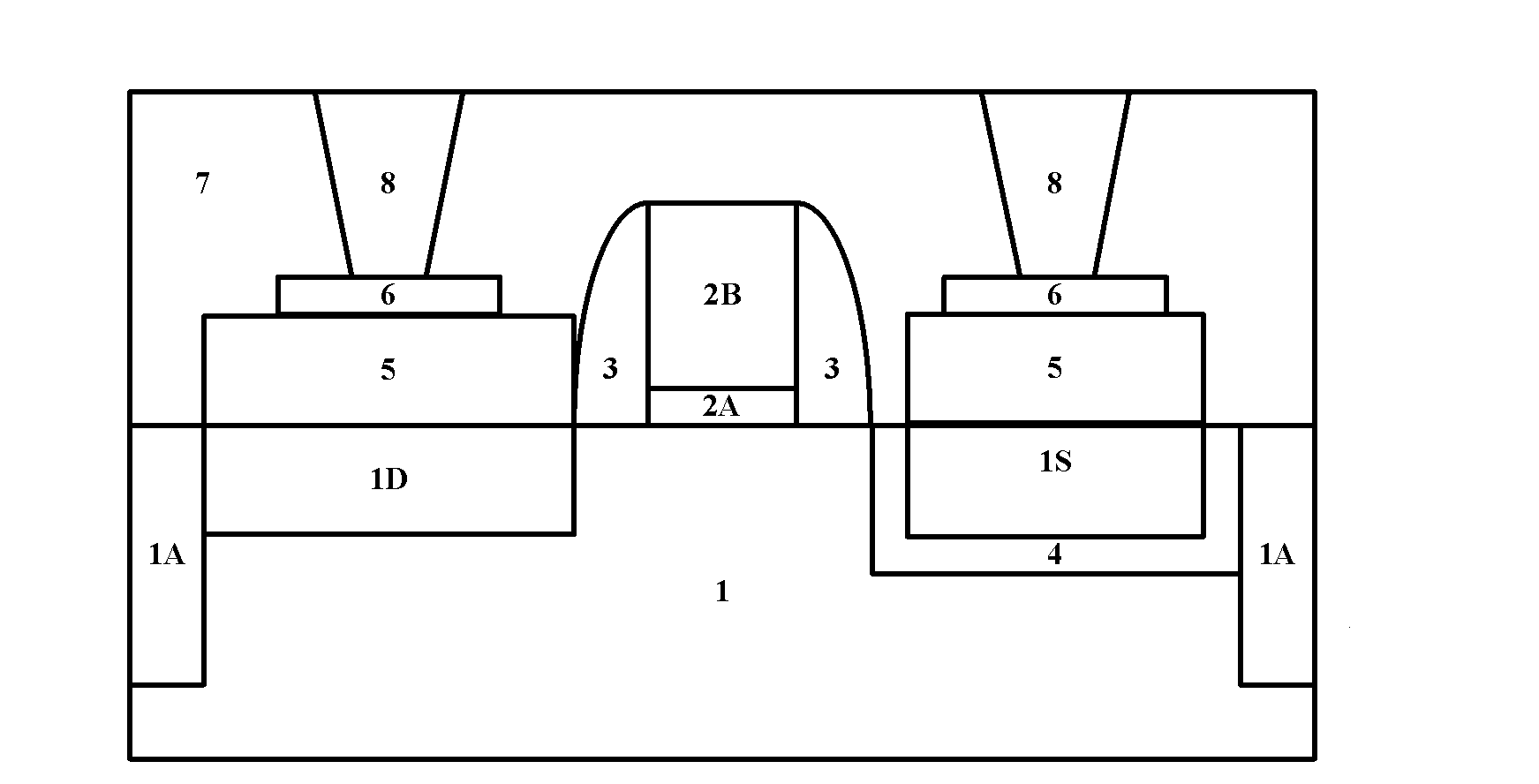
[0034]The features and the technical effects of the technical solution of the present application will be described in detail in combination with the illustrative embodiments with reference to the drawings. It should be pointed out that like reference signs indicate like structures, the terms such as “first”, “second”, “above”, “below”, “thickness” and “thin” used in the present invention may be used to describe various device structures. Except for specific explanations, these descriptions do not imply the spatial, sequential or hierarchical relationships of the structures of the described device.

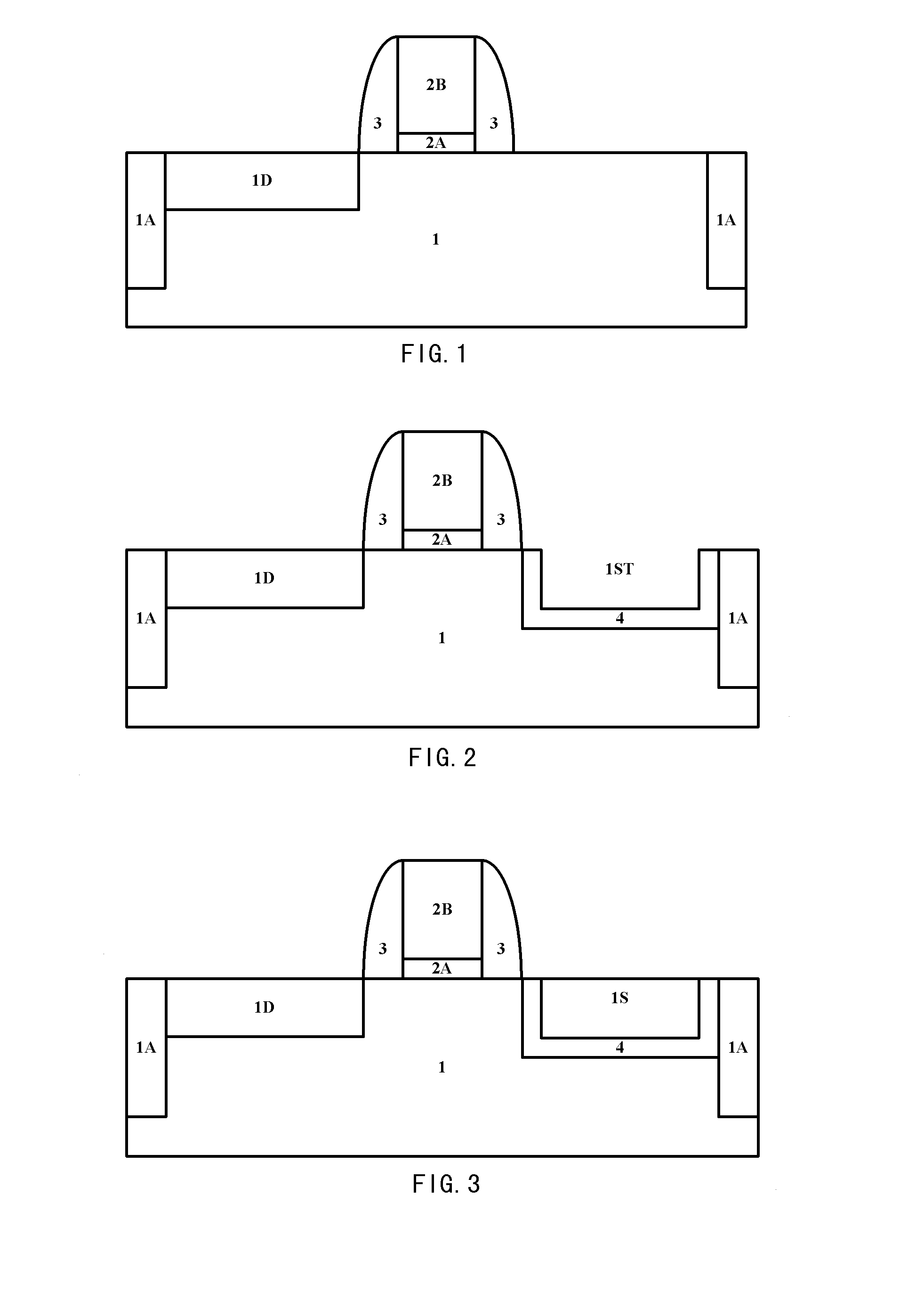
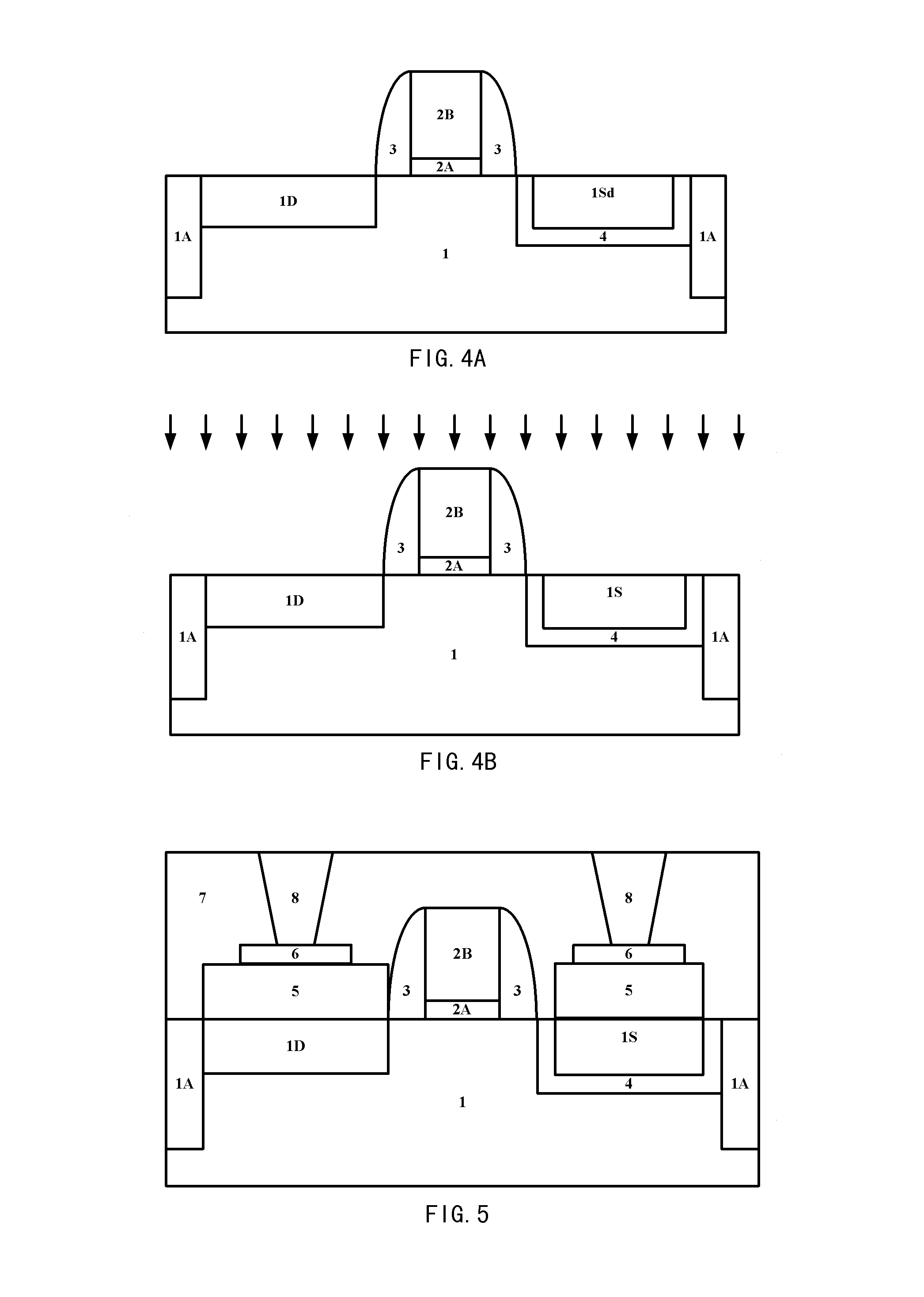
[0035]In accordance with a first embodiment of the present invention, referring to FIGS. 1 to 3, a conventional MOSFET device structure having a GeSn stressed source / drain region is formed.

[0036]First, referring to FIG. 1, a gate stack structure 2 and a gate spacer 3 are formed on a substrate 1, and a drain region 1D is formed by implantation in the substrate 1 at one side of the gate stac...


PUM


Abstract

The present invention discloses a semiconductor device, comprising: a substrate, a gate stack structure on the substrate, source and drain regions in the substrate on both sides of the gate stack structure, and a channel region between the source and drain regions in the substrate, characterized in that the source region in the source and drain regions comprises GeSn alloy, and a tunnel dielectric layer is optionally comprised between the GeSn alloy of the source region and the channel region. In accordance with the semiconductor device and method for manufacturing the same of the present invention, GeSn alloy having a narrow band gap is formed by implanting precursors and performing a laser rapid annealing, the on-state current of TFET is effectively enhanced, accordingly it has an important application prospect in a high performance low power consumption application.

Description

CROSS REFERENCE [0001]This application is a National Phase application of, and claims priority to, PCT Application No. PCT / CN2012 / 001377, filed on Oct. 12, 2012, entitled ‘SEMICONDUCTOR DEVICE AND METHOD FOR MANUFACTURING THE SAME’, which claimed priority to Chinese Application No. CN 201210293525.X, filed on Aug. 16, 2012. Both the PCT Application and Chinese Application are incorporated herein by reference in their entireties.FIELD OF THE INVENTION[0002]The present invention relates to the field of manufacturing of a semiconductor integrated circuit, in particular, to a tunnel field-effect transistor (TFET) with GeSn alloy as the source and a method for manufacturing the same.BACKGROUND OF THE INVENTION[0003]With the on-going development of the integrated circuit technology, particularly the continuous reduction of the device size in scale, various key parameters of the device such as the threshold voltage are also reduced accordingly, the advantages of reduction in the power cons...

Claims


Application Information

Patent Timeline
Patent Type & Authority Applications(United States)
IPC IPC(8): H01L29/78H01L29/66
CPCH01L29/66477H01L29/78H01L21/26506H01L29/41783H01L29/456H01L29/66356H01L29/66659H01L29/7391H01L29/7835H01L29/7848H01L29/161H01L29/165H01L29/0895
Inventor MA, XIAOLONGYIN, HUAXIANGFU, ZUOZHEN
Owner INST OF MICROELECTRONICS CHINESE ACAD OF SCI
Why Eureka
Try Eureka