Display device and driving method thereof

a technology of a display device and a driving method, which is applied in the direction of semiconductor devices, electrical devices, instruments, etc., can solve the problems of unfitness for displaying moving images, high manufacturing cost of a passive matrix drive, and inability to large-area or high-definition display devices, etc., to achieve the effect of increasing data current, increasing aperture ratio, and increasing aperture ratio

Active Publication Date: 2011-06-28
SEMICON ENERGY LAB CO LTD
View PDF31 Cites 166 Cited by
  • Summary
  • Abstract
  • Description
  • Claims
  • Application Information

AI Technical Summary

Benefits of technology

[0018]In view of the foregoing problems, the present invention provides a current input type pixel circuit, which has shorter program time and high aperture ratio of a pixel.
[0039]As described above, a threshold holding capacitor Ct is replaced by capacitance Cel of a display element; therefore, a data current may be increased compared to a drive current of the display element without providing Ct. In addition, an aperture ratio can be increased because Ct is not provided in a pixel. When the aperture ratio is high, the capacitance Cel of the display element becomes large; therefore, a data current may be further increased. In this manner, an increase in aperture ratio leads to an increase in data current, which generates a synergistic and significant effect.

Problems solved by technology

However, when one pixel is driven, other pixels cannot be driven so that it is not good for a large-area or high-definition display device.
On the other hand, an active matrix drive has an active element and a unit for holding luminance data in each pixel, so that manufacturing cost is higher than a passive matrix drive.
A liquid crystal display has been spread widely, but has problems such as unfitness for displaying a moving image because of slow response speed, and dependence on viewing angle.
In addition, a display element is not self-light emitting type; therefore, a back light is required so that power consumption is high.
This nature mainly causes a problem of an organic EL element driven by an active matrix drive.
However, when a current value of a display element is very small when driven display element such as an organic EL element, there is a problem in that time (also referred to as program time) for charging the capacitor Cs becomes very long since a data current corresponds one-to-one to a current value of the display element 10 when driven in the circuit shown in FIG. 8.

Method used


Image

  • Display device and driving method thereof
  • Display device and driving method thereof
  • Display device and driving method thereof

Examples


embodiment mode 1

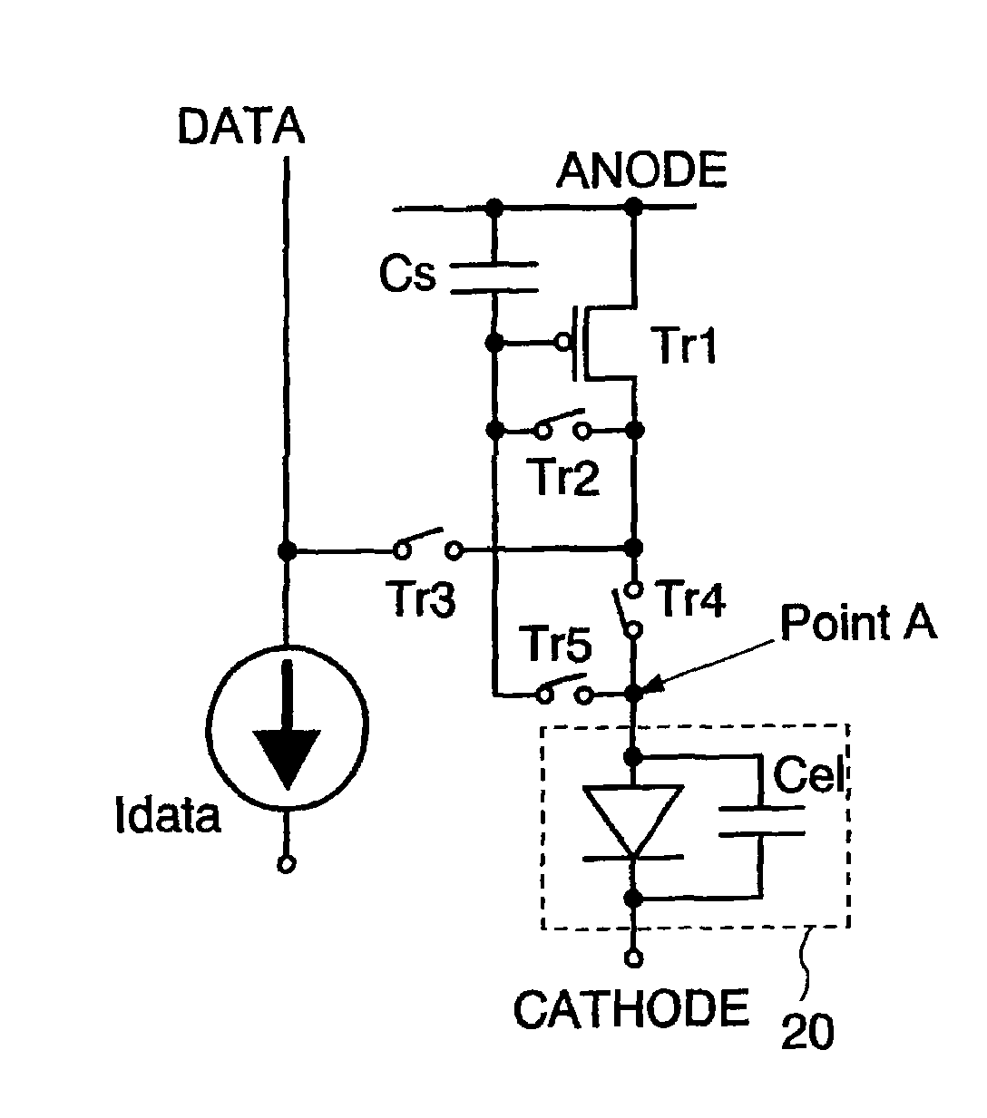
[0060]In this embodiment mode, first, description is made of a display device of the invention with reference to FIG. 3. The display element of the invention includes a data line driver circuit 302 as a peripheral driver circuit, a scan line driver circuit 303, n data lines (X1 to Xn) (n is an integer) driven by the data line driver circuit 302, m scan lines (Y1 to Ym) (m is an integer) driven by the scan line driver circuit 303, a plurality of pixel circuits 304 arranged in a position where the m scan lines (m is more than one) and the n data lines cross, and a pixel portion 301 including the plurality of pixel circuits 304. A selection signal is transmitted by the scan lines, and a data current for showing an image signal flows through the data lines. Note that although FIG. 3 shows a case where one pixel circuit 304 is provided with one data line and one scan line, the invention is not limited to this, and one pixel circuit 304 may be provided with a plurality of scan lines and d...

embodiment mode 2

[0094]Next, description is made of a second mode of a display device of the invention with reference to FIGS. 4A, 4B, and 5.

[0095]A pixel circuit in this embodiment mode may be applied to FIG. 1 explained in Embodiment Mode 1. Note that in this embodiment mode a manufacturing method of the second power supply line CATHODE is different from the mode explained in Embodiment Mode 1, which can generate a particular effect. Description is made of a mode of the second power supply line CATHODE with reference to FIGS. 4A and 4B.

[0096]FIG. 4A is a schematic view of the second power supply line CATHODE in the display device explained in the aforementioned Embodiment Mode 1. The second power supply line CATHODE in FIG. 4A has a mode of being connected to all pixel circuits in common as already described in Embodiment Mode 1. A pixel portion 301 is formed over a substrate 401, over which an EL element is formed as a display element, over which a contact region 402 with a lower electrode is for...

embodiment mode 3

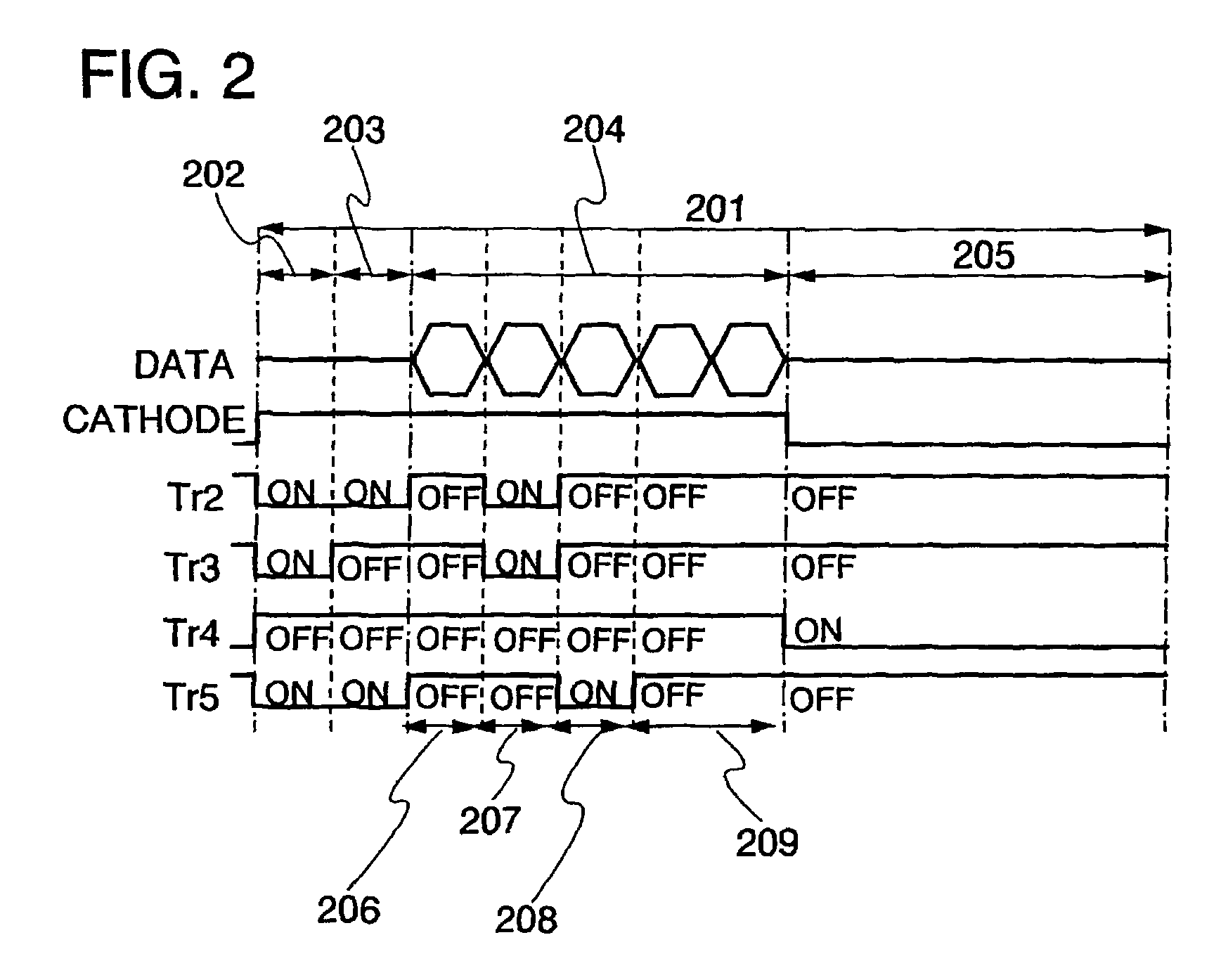
[0106]Next, description is made of a third mode of a display device of the invention with reference to FIG. 6. In this embodiment mode, a driving method of the display device by alternating a first power supply line ANODE is described. In this embodiment mode, a second power supply line CATHODE may be connected to all pixels in common, which is described in this embodiment mode. However, the second power supply line CATHODE may be processed in shape in this embodiment mode.

[0107]In FIG. 6, an input signal is described in the case where the display device of the invention is driven by alternating the first power supply line ANODE with polarity of all transistors being p-channel. One frame includes the initialization period 202, the threshold writing period 203, the address period 204, the light emitting period 205, which is the same as the drive shown in Embodiment Mode 1, and a performance of circuits in each period is almost the same as well. Therefore, in this embodiment mode, des...


PUM


Abstract

To solve the lack of program time, which is a problem of a display device including an EL element, and to provide a display device including a pixel circuit with a high aperture ratio and a driving method thereof. In a circuit including a driving transistor, a capacitor, a display element which can be used as a capacitor, a first power supply line and a second power supply line, potentials of the first power supply line and the second power supply line are set to be almost the same, thereby a threshold voltage of the driving transistor is held in the display element, and after that, a charge is divided into the display element and the capacitor.

Description

TECHNICAL FIELD[0001]The present invention relates to a display device to which a self-light emitting type display element is applied and a driving method thereof.BACKGROUND ART[0002]In a driving method of a display device, there are an active matrix drive and a passive matrix drive mainly. A passive matrix drive has a structure that a display element is sandwiched between electrodes arranged in matrix, which can be manufactured at low cost. However, when one pixel is driven, other pixels cannot be driven so that it is not good for a large-area or high-definition display device. On the other hand, an active matrix drive has an active element and a unit for holding luminance data in each pixel, so that manufacturing cost is higher than a passive matrix drive. However, while one pixel is driven, other pixels can emit light holding luminance data. Therefore, an active matrix driving method is used for most of large-area or high-definition display devices.[0003]An active matrix display ...

Claims


Application Information

Patent Timeline
Patent Type & Authority Patents(United States)
IPC IPC(8): G09G3/30
CPCG09G3/325G09G2300/0417G09G2300/0465G09G2300/0809G09G2300/0852G09G2300/0866H01L2251/5323G09G2320/0223G09G2320/043G09G2330/08H01L27/3211H01L27/3244H01L51/0011G09G2310/0256H10K59/35H10K59/12H10K71/166H10K2102/3031H01L2027/11879
Inventor YOSHIDA, YASUNORI
Owner SEMICON ENERGY LAB CO LTD
Why Eureka
Try Eureka