

Semiconductor light emitting device
a technology of light-emitting elements and semiconductors, which is applied in the direction of semiconductor devices, basic electric elements, electrical appliances, etc., can solve the problems of insufficient light extraction efficiency, limited light extraction efficiency improvement, and relatively thick pad electrodes, etc., to achieve improved ohmic characteristics, improved light extraction efficiency, and reduced schottky barriers.
- Summary
- Abstract
- Description
- Claims
- Application Information
AI Technical Summary
Benefits of technology
Problems solved by technology
Method used
Image

Examples
example 1
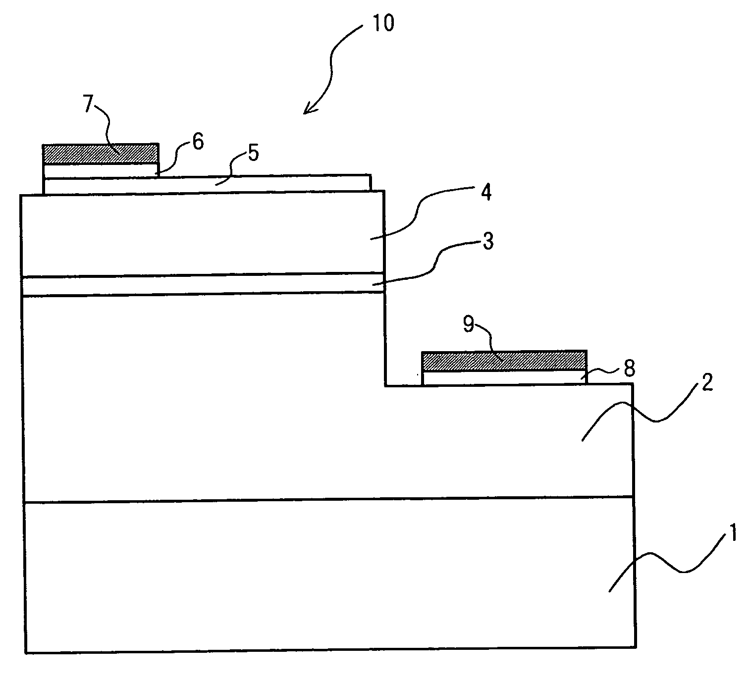
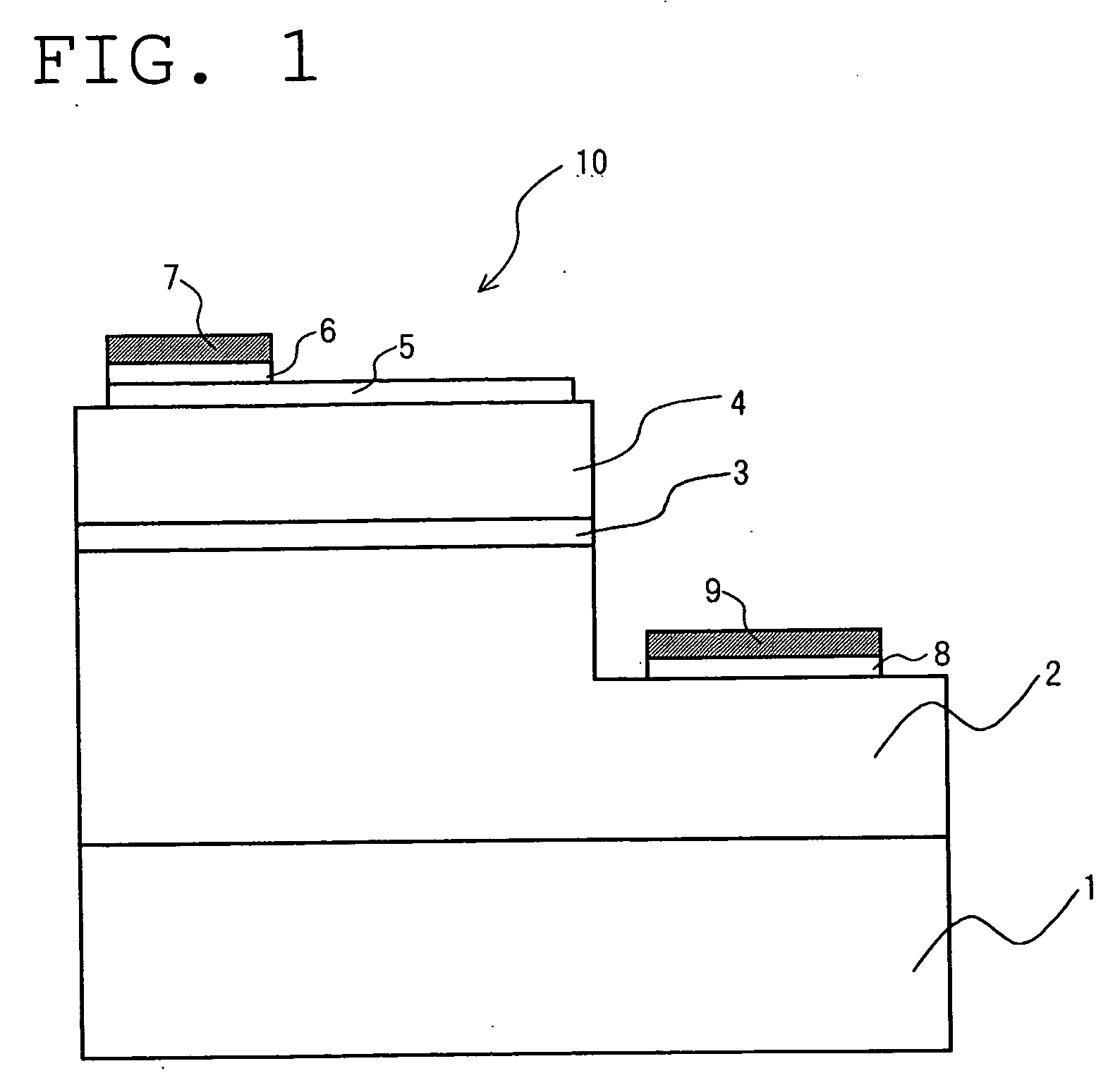
[0172] A semiconductor light emitting device of this example is shown in FIG. 1.
[0173] The semiconductor light emitting device 10 is formed by stacking, in this order, onto a sapphire substrate 1, a buffer layer (not shown in the figures) made of Ai0.1Ga0.9N and an undoped GaN (not shown in the figures). On top of that are stacked an n-type contact layer made of Si doped GaN and a superlattice n-type cladding layer in which a GaN layer (40 Å) and a InGaN layer (20 Å) are alternately stacked ten times as an n-type semiconductor layer 2. On top of that are stacked an active layer 3 having a multiquantum well structure in which a GaN layer (250 Å) and an InGaN layer (30 Å) are alternately stacked three to six times, and then, stacked thereon are a superlattice p-type cladding layer in which Al0.1Ga0.9N layer doped with Mg (40 Å) and InGaN layer doped with Mg (20 Å) are alternately laminated ten times, as a p-type semiconductor layer 4.
[0174] A p-side electrode is disposed on the p-ty...
example 2
[0194] The semiconductor light emitting device of this example is fabricated in the same manner as in Example 1, except that the metal film of the p-side electrode and the metal film of the n-side electrode are disposed in the separate steps.
[0195] A mask of a resist having a predetermined pattern is disposed on the upper ITO film 6, and the metal film 7 made of Rh(1000 Å) / Pt(2000 Å) / Au(5000 Å) is formed thereon.
[0196] Then, the metal film 7 comprising a W layer of 200 Å, a Pt layer of 2000 Å, and an Au layer of 5000 Å stacked in this order is disposed on the ITO film 8 that is disposed on the b-side contact layer.
[0197] A semiconductor light emitting device obtained in this manner has a similar effect as in Example 1.
[0198] As described above, according to the structure of the semiconductor light emitting device of the present invention, the adhesion between the positive electrode and the p-side contact layer and between the n-side electrode and the n-side contact layer can be ...
example 3
[0199] As shown in FIG. 5, in the semiconductor light emitting device of the present example, the p-side electrode 20 and the n-side electrode 19 are provided in the same surface side. The semiconductor light emitting device has a construction, in which the light is extracted from the electrode forming surface side as an observation side. The layered structure of semiconductor in the semiconductor light emitting device comprises a GaN buffer layer 12, a undoped GaN layer 13, an Si-doped GaN layer 14 as an n-side contact layer, an Si-doped GaN layer 15 as an n-type cladding layer, an InGaN layer 16 as a light emitting layer, a Mg-doped GaN layer 18 as p-side contact layer are successively stacked on a sapphire substrate 1. Furthermore, the Mg-doped GaN layer 18, the Mg-doped AlGaN layer 17, the InGaN layer 16, the Si-doped GaN layer 15, and the Si-doped GaN layer 14 are partially removed by etching etc., the n-side electrode 19 is disposed on the exposed surface of the Si-doped GaN l...
PUM
 Abstract
Description
Claims
Application Information