Variable initial program voltage magnitude for non-volatile storage

a non-volatile storage and variable initial program technology, applied in the field of non-volatile storage, can solve the problem of increasing the time needed for programming and the same, and achieve the effect of improving the programming speed

US7564715B2Active Publication Date: 2009-07-21SANDISK TECH LLC
49 Cites 19 Cited by

Patent Information

Authority / Receiving Office
US · United States
Patent Type
Patents(United States)
Current Assignee / Owner
Publication Date
2009-07-21

Smart Images

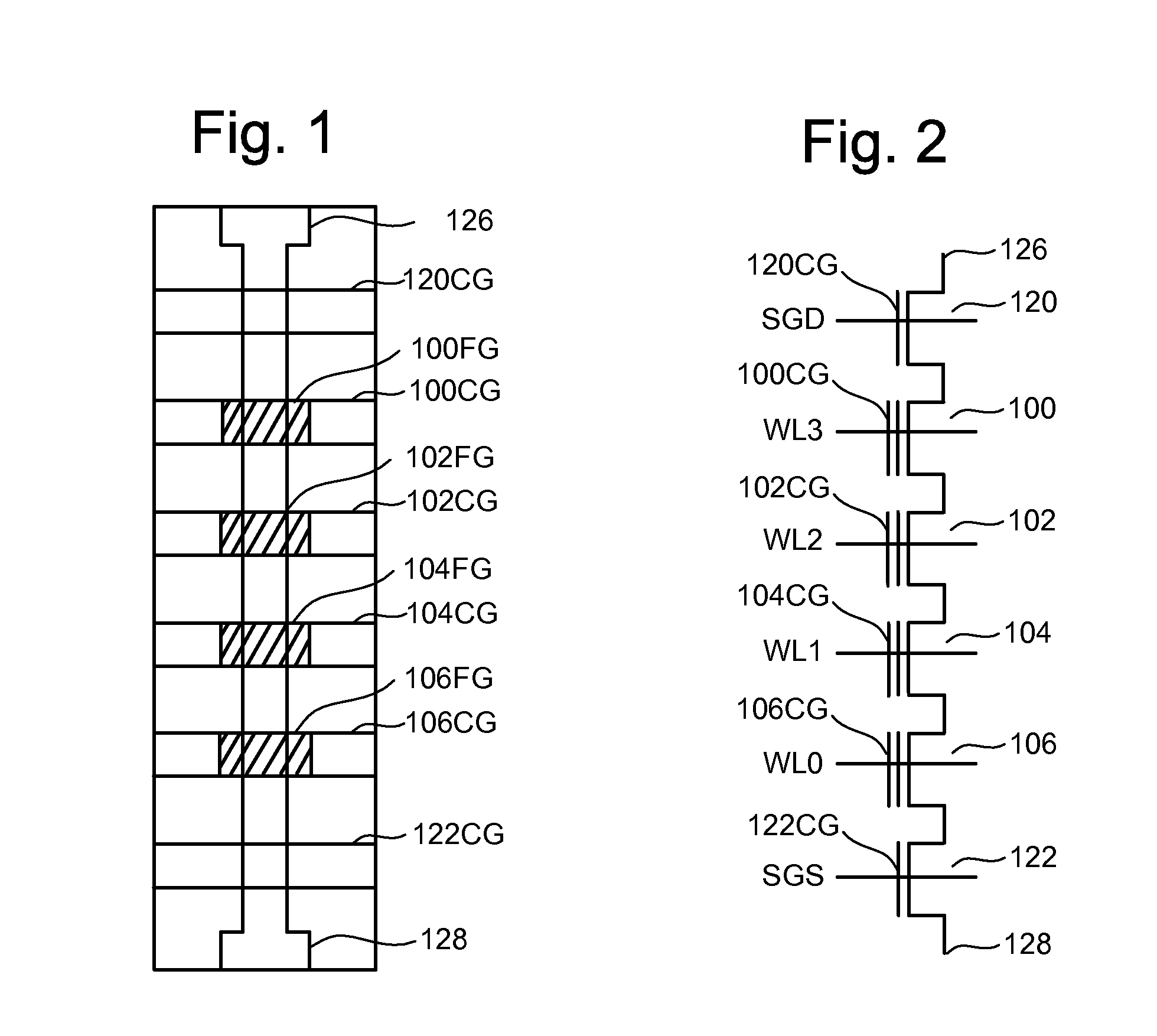
  • Figure 1
    Figure 1
  • Figure 2
    Figure 2
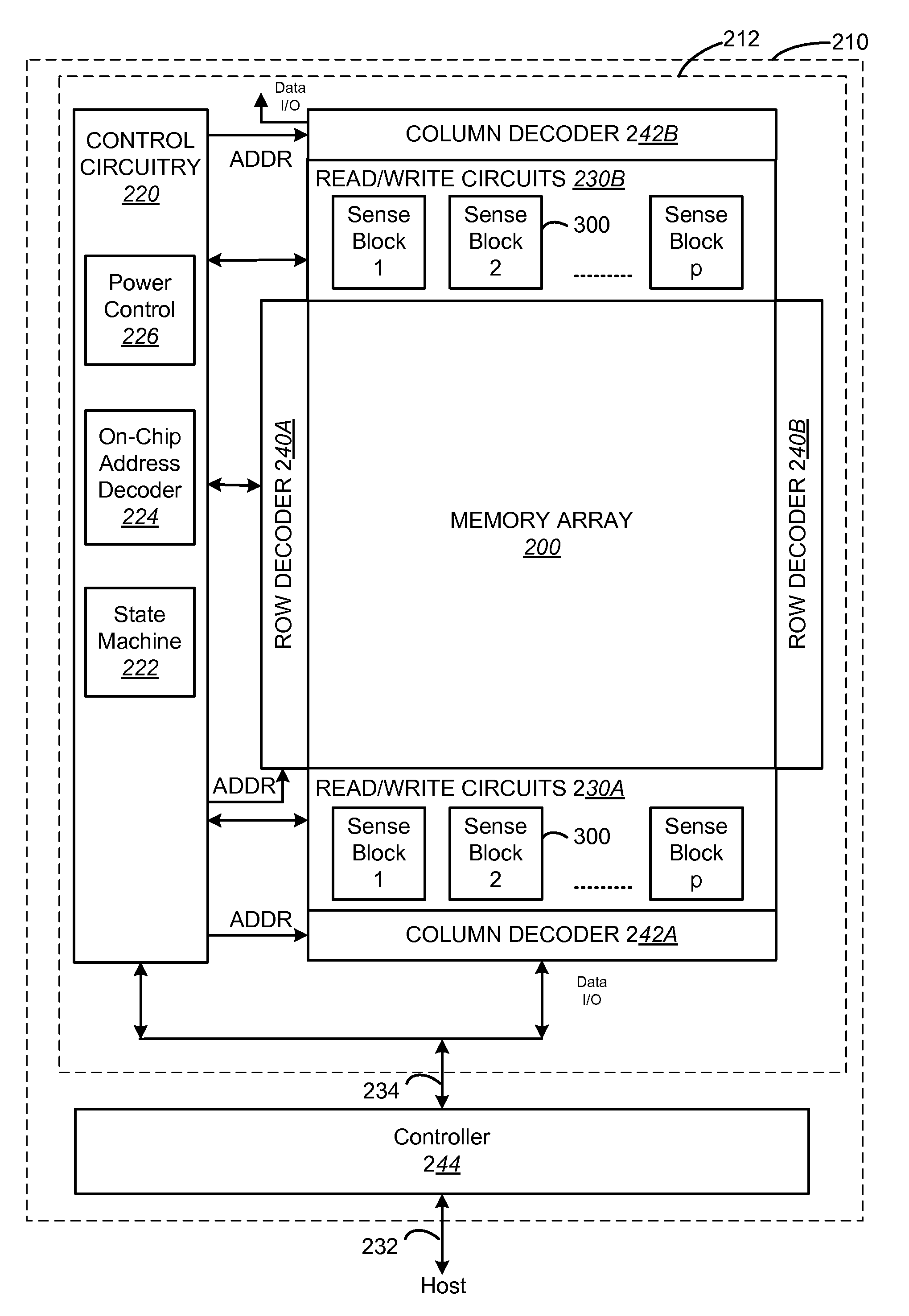
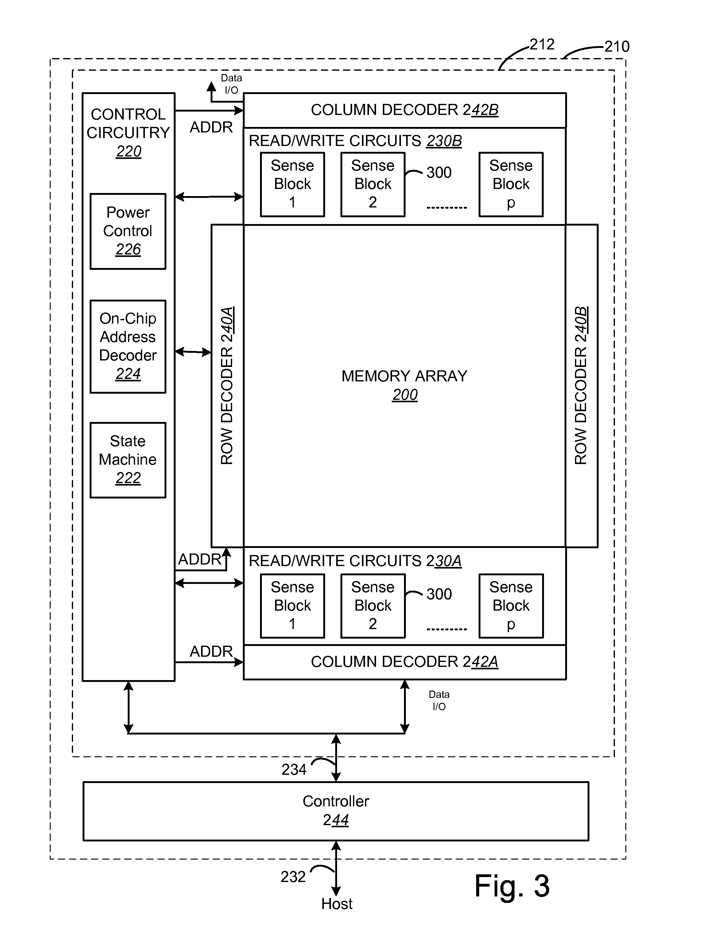
  • Figure 3
    Figure 3
Patent Text Reader

Abstract

Multiple programming processes are performed for a plurality of non-volatile storage elements. Each of the programming process operates to program at least a subset of said non-volatile storage elements to a set of target conditions using program pulses. In one embodiment, a first programming pass includes soft programming and additional programming passes include the programming of data. In another embodiment, all of the programming process include programming data. For at least a subset of said programming processes, a program pulse associated with achieving a particular result for a respective programming process is identified. The identified program pulse is used to adjust programming for a subsequent programming process.
Need to check novelty before this filing date? Find Prior Art

Description

[0001] This application claims the benefit of provisional application No. 60 / 890,832, “Diagonal Sequence Write,” by Nima Mokhlesi, filed on Feb. 20, 2007, incorporated herein by reference in its entirety.CROSS-REFERENCE TO RELATED APPLICATIONS

[0002] The following applications are cross-referenced and incorporated by reference herein in their entirety: U.S. patent application Ser. No. 11 / 694,987, published as U.S. Patent Publication No. 20080198660, titled “Multiple Pass Write Sequence For Non-Volatile Storage” Inventor Nima Mokhlesi, filed Mar. 31, 2007; U.S. patent application Ser. No. 11 / 694,989, published as U.S. Patent Publication No. 200800198664, titled “Non-Volatile Storage Apparatus With Multiple Pass Write Sequence,” Inventor Nima Mokhlesi, filed Mar. 31, 2007; U.S. patent application Ser. No. 11 / 694,991, published as U.S. Patent Publication No. 20080198661, titled “Non-Volatile Storage Apparatus With Variable Initial Program Voltage Magnitude,” Inventor Nima Mokhlesi, filed ...

Examples

Embodiment Construction

[0040]One example of a flash memory system uses the NAND structure, which includes arranging multiple transistors in series, sandwiched between two select gates. The transistors in series and the select gates are referred to as a NAND string. FIG. 1 is a top view showing one NAND string. FIG. 2 is an equivalent circuit thereof. The NAND string depicted in FIGS. 1 and 2 includes four transistors 100, 102, 104 and 106 in series and sandwiched between a first (or drain side) select gate 120 and a second (or source side) select gate 122. Select gate 120 connects the NAND string to a bit line via bit line contact 126. Select gate 122 connects the NAND string to source line 128. Select gate 120 is controlled by applying the appropriate voltages to select line SGD. Select gate 122 is controlled by applying the appropriate voltages to select line SGS. Each of the transistors 100, 102, 104 and 106 has a control gate and a floating gate. For example, transistor 100 has control gate 100CG and ...