Method and device for carrying out data programming on flash

A data programming and data technology, which is applied in the field of memory, can solve problems affecting programming speed, etc., and achieve the effects of increasing programming speed, reducing switching times, and saving charging and discharging time

Active Publication Date: 2010-08-11
GIGADEVICE SEMICON SHANGHAI INC +1
View PDF0 Cites 15 Cited by
  • Summary
  • Abstract
  • Description
  • Claims
  • Application Information

AI Technical Summary

Problems solved by technology

Due to the large number of voltage switching times in the prior art, the charge and discharge time add up to be considerable, which seriously affects the programming speed

Method used


Image

  • Method and device for carrying out data programming on flash
  • Method and device for carrying out data programming on flash
  • Method and device for carrying out data programming on flash

Examples


Embodiment 1

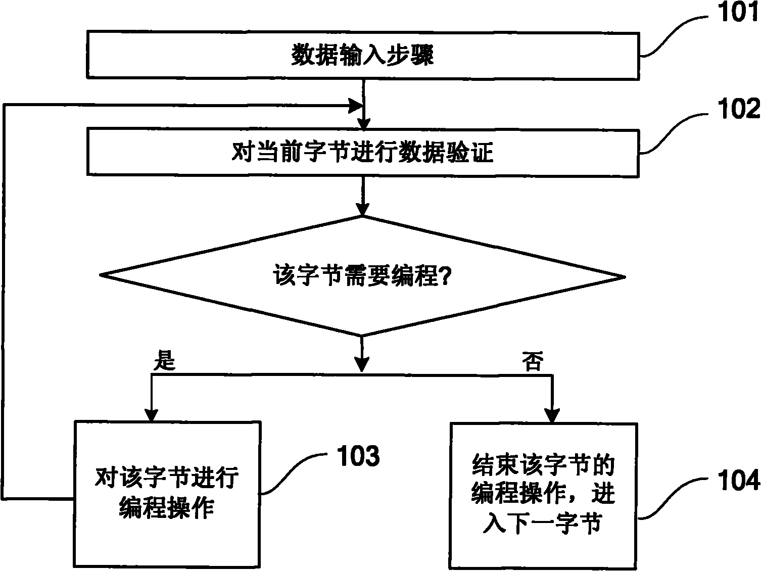
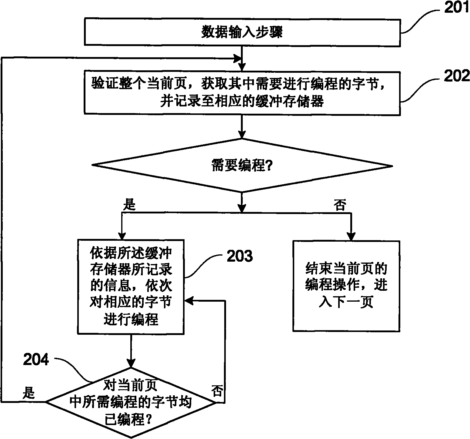
[0046] refer to figure 2 , showing a method embodiment 1 for performing data programming on a flash memory, which is characterized in that it includes:

[0047] Step 201, the data input step; more specifically, the received data (that is, the data to be written) can be stored in the page buffer of the flash memory, so as to be acquired in the subsequent programming step;

[0048] Step 202, verify the entire current page, obtain the bytes that need to be programmed, and record them into the corresponding buffer memory; if there are no bytes that need to be programmed in the current page, then end the data programming operation of the current page, and enter the next page. one page;

[0049] Of course, it should be noted that when all the input data has been programmed, there is no need to enter the verification and programming process on the next page, and the entire programming operation can be ended directly.

[0050] Step 203, according to the information recorded in the bu...

Embodiment 2

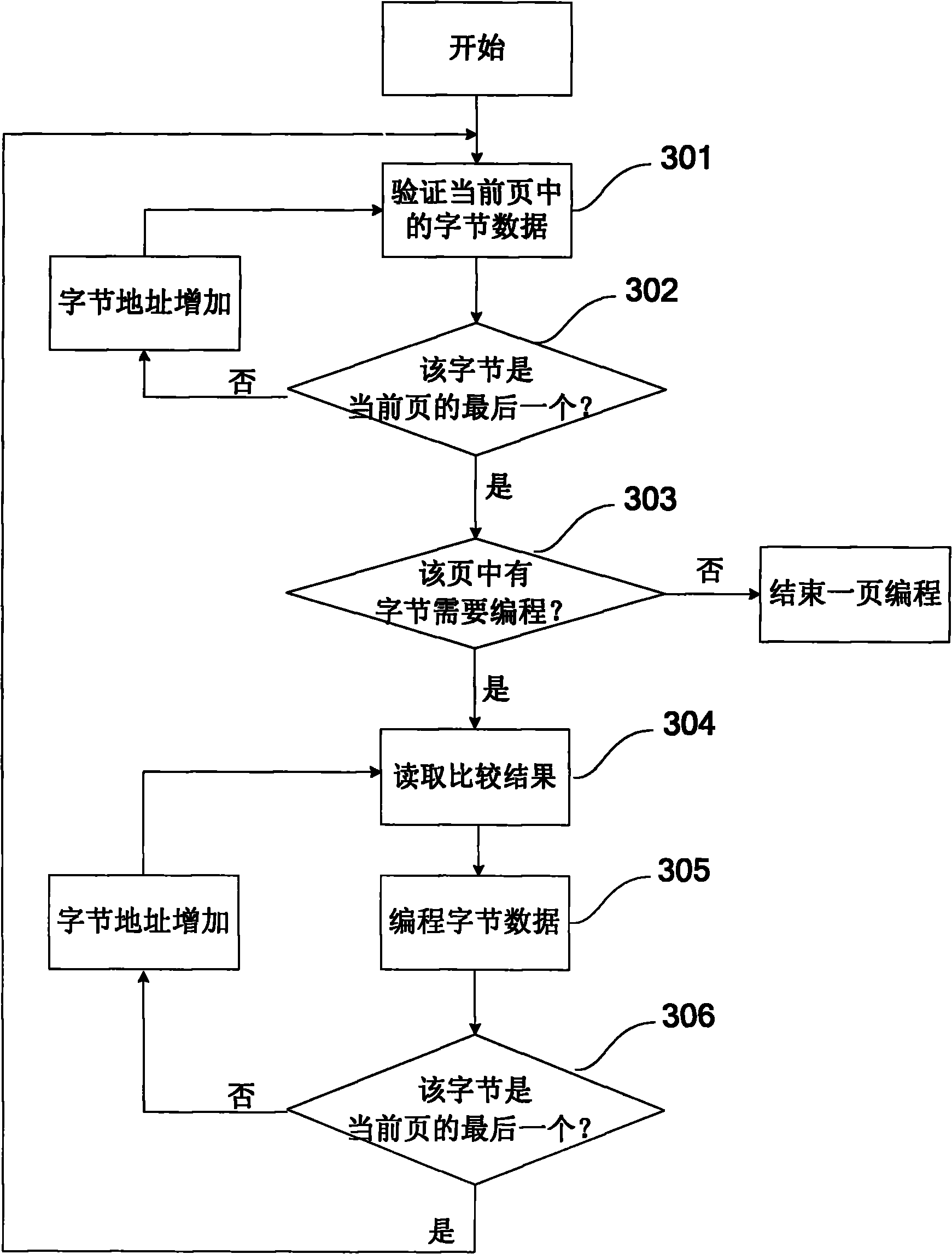
[0060] refer to image 3 , shows an embodiment 2 of the present invention for performing data programming on a flash memory, which may specifically include:

[0061] Step 301, starting from the start address of a page, verifying in units of bytes, comparing whether the data stored in the byte is consistent with the data to be written; writing the result into the buffer memory corresponding to the byte address ; Of course, generally, a byte does not correspond to a buffer memory, and the comparison result of the byte can be stored in the buffer memory corresponding to the address of the byte.

[0062] Step 302 , after verifying the current byte, increase the byte address, and verify the byte at the next address until the entire page is verified. Specifically, it can be judged whether the currently verified byte is the last byte of the page, and if yes, the next step is performed; otherwise, the byte address is increased to continue the verification.

[0063] Step 303 , confir...


PUM


Abstract

The invention discloses a method for carrying out data programming on flash, comprising the following steps: a. inputting data; b. verifying the current whole page, obtaining the bytes needing to be programmed in the page and recording the bytes into a corresponding buffer storage unit, and completing data programming in the current page if the current page contains no bytes needing to be programmed; and c. programming the corresponding bytes in sequence according to the information recorded in the buffer storage unit, and if the bytes needing to be programmed in the current page have been programmed, returning to the step b, or continuing the step c and operating the next byte. In the invention, the step of data verification and the step of data writing in the process of programming operation are carried out on the whole page, thus greatly reducing the switching times of different voltage on loading grid and drain, saving the charge and discharge time of the grid and drain voltage pumps and then improving the programming speed of flash.

Description

technical field [0001] The invention relates to the technical field of memory, in particular to a method and device for programming data in flash memory. Background technique [0002] A flash memory (Flash) is a storage device for storing data, and has a characteristic (non-volatile) that data remains unerased even if power supply is stopped. For this reason, flash memory has been used as a data storage device of electronic products such as mobile phones, PDAs, and MP3 players, and has a tendency to be more and more widely used. [0003] Generally speaking, Flash can be divided into NOR-type Flash and NAND-type Flash. What they have in common is that data is stored (data written) by a program operation and erased by an erase operation. Both are voltage-controlled devices. The erasing and writing of NAND Flash are based on the tunnel effect. The current passes through the insulating layer between the floating gate and the silicon base layer to charge the floating gate (writ...

Claims


Application Information

Patent Timeline
Patent Type & Authority Applications(China)
IPC IPC(8): G11C16/10G11C16/34
Inventor 潘荣华
Owner GIGADEVICE SEMICON SHANGHAI INC
Why Eureka
Try Eureka