Substrate bias for programming non-volatile memory

Active Publication Date: 2006-04-04
MONTEREY RES LLC
View PDF5 Cites 18 Cited by
  • Summary
  • Abstract
  • Description
  • Claims
  • Application Information

AI Technical Summary

Benefits of technology

[0021]Embodiments of the present invention provide a means to increase the programming speed of flash memory. Further embodiments of the present invention provide for increasing the programming speed of flash memory in a manner that is compatible and complimentary with convention

Problems solved by technology

Silicon-Oxide-Nitride-Oxide-Silicon (SONOS) is potentially very dense in terms of number of cells per unit area that can be used and it requires fewer process steps as compared to floating gate memory.
Memory device manufacturers are continually challenged to provide ever greater amounts of memory at ever lower costs.
However, flash memory generally can not be written to, or programmed, at rates comparable to random access memory, RAM, or at rates directly compatible with a computer system's processing unit.
Consequently, the benefits of flash, e.g., changeable non-volatile storage, demand a deleterious decrease in write performance of the memory subsystem.
In addition, as most computer systems utilizing flash memory also employ RAM, the complexities of managing the differing timing requirements between flash and RAM are an undesirable burden on system designers seeking to utilize flash memory.
This is a disadvantage compared to RAM and hard drives, which may be written directly, without an interposing erasure.
The use of additional software, e.g., a

Method used


Image

  • Substrate bias for programming non-volatile memory
  • Substrate bias for programming non-volatile memory
  • Substrate bias for programming non-volatile memory

Examples


Embodiment Construction

[0027]In the following detailed description of the present invention, substrate bias for programming non-volatile memory, numerous specific details are set forth in order to provide a thorough understanding of the present invention. However, it will be recognized by one skilled in the art that the present invention may be practiced without these specific details or with equivalents thereof. In other instances, well-known methods, procedures, components, and circuits have not been described in detail so as not to unnecessarily obscure aspects of the present invention.

Substrate Bias for Programming Non-Volatile Memory

[0028]Embodiments of the present invention are described in the context of design and operation of flash memory devices. However, it is appreciated that embodiments of the present invention may be utilized in other areas of electronic design and operation.

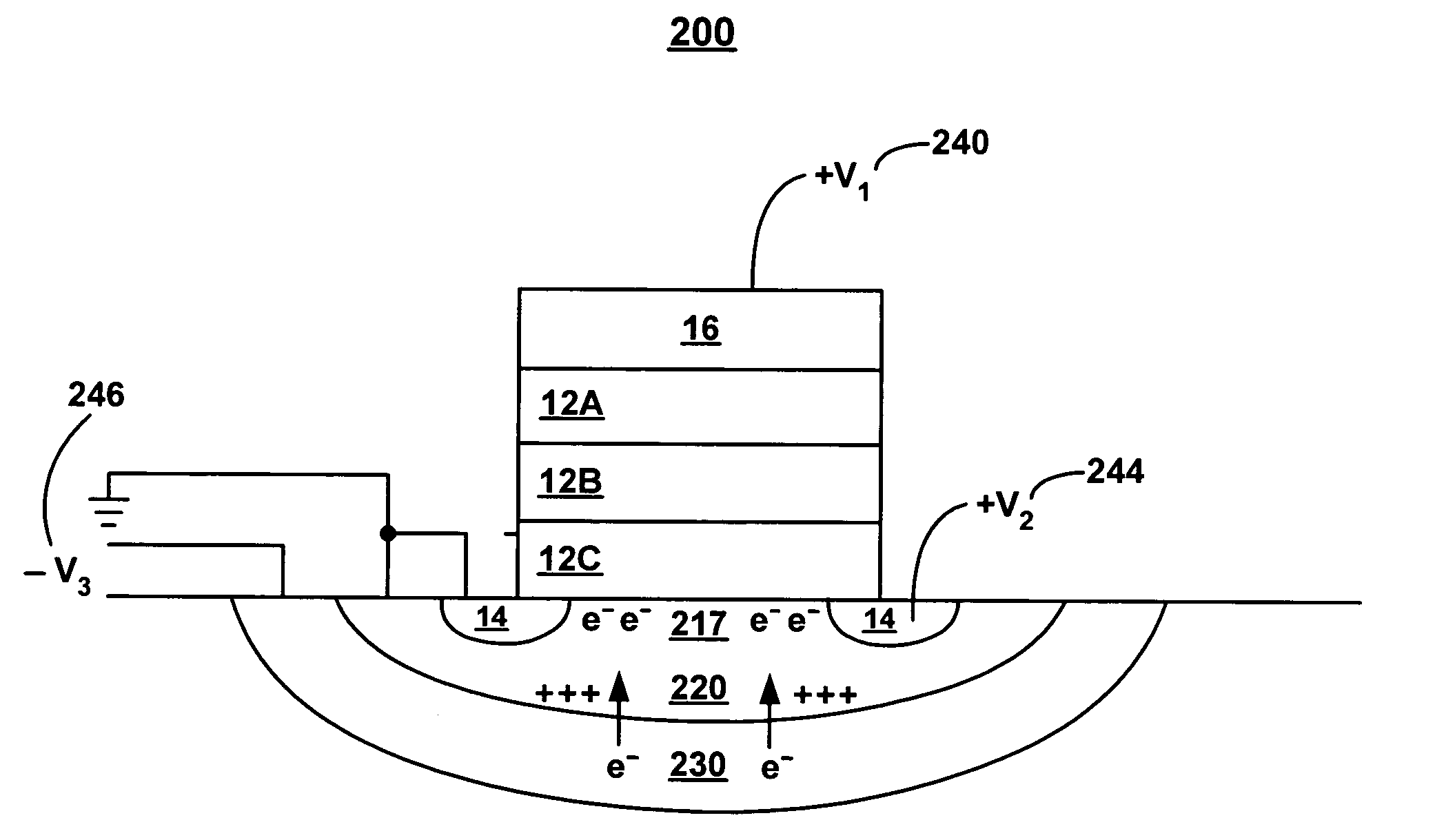
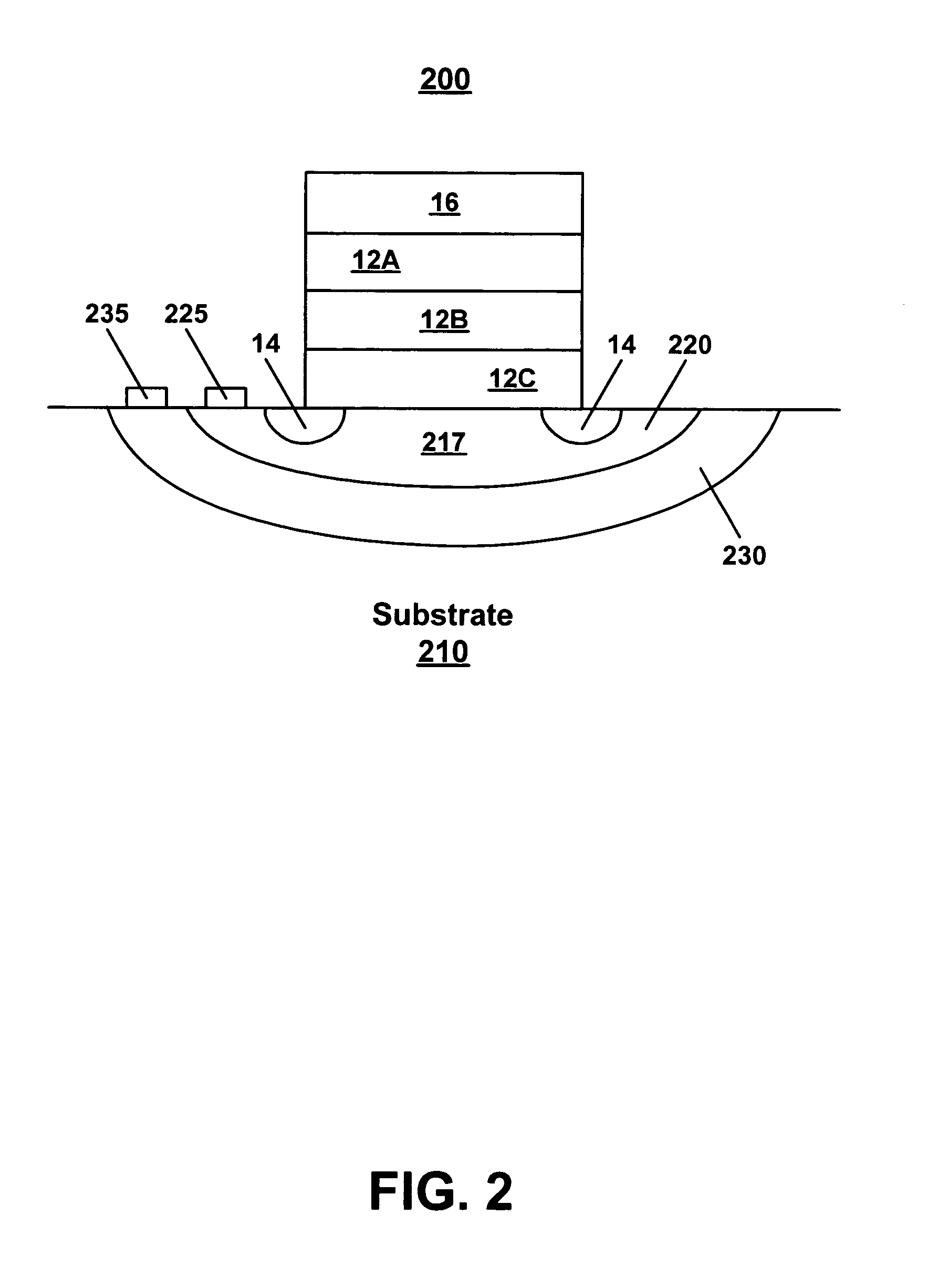
[0029]FIG. 2 illustrates a non-volatile memory cell 200, according to an embodiment of the present invention. Regions ...


PUM


Abstract

A method and system for substrate bias for programming non-volatile memory. A bias voltage is applied to a deep well structure under a well comprising a channel region for a non-volatile memory cell. During programming, a negative bias applied to the deep well beneficially creates a non-uniform distribution of electrons within the channel region, with an abundance of electrons at the surface of the channel region. The application of additional bias voltages to a control gate and a drain may cause electrons to migrate from the channel region to a storage layer of the non-volatile memory cell. Advantageously, due to the increased supply of electrons at the surface of the channel region, programming of the non-volatile cell takes place faster than under the conventional art.

Description

TECHNICAL FIELD[0001]Embodiments of the present invention relate to design and operation of sub-micron metal oxide semiconductors. More particularly, embodiments of the present invention provide a substrate bias for programming non-volatile memory.BACKGROUND ART[0002]Flash memory is a type of semiconductor computer memory with many desirable characteristics. Like read only memory, ROM, it is non-volatile, meaning that the contents of the memory are stable and retained without applied electrical power.[0003]Flash memory devices have found wide commercial success in the electronic device market. A major advantage of flash over ROM is that the memory contents of flash may be changed after the device is manufactured. Flash memory has found wide acceptance in many types of computers, including desktop computers, mobile phones and hand held computers. Flash memory is also widely used in digital cameras and portable digital music players, for example “MP3” players.[0004]In addition to dire...

Claims


Application Information

Patent Timeline
IPC IPC(8): G11C16/04
CPCG11C16/10
Inventor WONG, NGA-CHINGHAMILTON, DARLENE G.
Owner MONTEREY RES LLC
Why Eureka
Try Eureka