Single crystal fuse on air in bulk silicon

a technology of fuse elements and silicon, applied in the direction of semiconductor devices, semiconductor/solid-state device details, resistors, etc., can solve the problems of sensitive transistor gate stacks at risk of damage, electronic systems often require functions to be enabled, disabled or modified, and fuse blowing may sometimes be unreliable, so as to improve the programming speed of integrated fuse devices and improve the temperature gradient

Active Publication Date: 2009-04-09
TWITTER INC
View PDF8 Cites 15 Cited by
  • Summary
  • Abstract
  • Description
  • Claims
  • Application Information

AI Technical Summary

Benefits of technology

[0018]It is a further object of the present invention to provide an integrated eFUSE device that produces an improved temperature gradient (for purposes of electromigration) compared to prior-art eFUSE devices.
[0019]It is a further object of the present invention to improve programming speed of integrated eFUSE devices.
[0020]It is a further object of the present invention to produce an integrated eFUSE device that requires reduced programming current and smaller programming transistors than prior-art eFUSE devices.
[0021]It is a further object of the present invention to reduce heat transfer from the eFUSE device into surrounding structures during programming.
[0022]It is a further object of the present invention to improve predictability of electromigration in programming eFUSE devices.

Problems solved by technology

However, if the conductive fuse link material is not sufficiently dispersed within the surrounding area, conductive debris or “fallout” from the “blow” process may still represent a conductive path even after the fuse device is blown.
In other words, especially with electrically blown fuses, the fuse “blow” may sometimes be unreliable.
Electronic systems often require functions to be enabled, disabled or modified after semiconductor chips used in the electronic systems have been manufactured.
In yet another example, static charges built up during certain processing steps in the fabrication and processing of dynamic random access memory (DRAM) circuits put sensitive transistor gate stacks at risk of damage.
Subsequently, whenever the defective address is accessed, the fuses and associated redundancy logic cause redundant cells to be accessed instead of the defective cells.
In some applications, the eFUSE is blown even after an electronic system utilizing the chip has been in operation for some time.
Present eFUSE devices typically lie on STI (shallow trench isolation) oxide, which provides reasonably good thermal isolation of the fuse device (compared to other materials in the chip), but which is still thermally conductive enough to present challenging tradeoffs in choosing the appropriate amount of thermal energy to use in blowing the EFUSE.

Method used


Image

  • Single crystal fuse on air in bulk silicon
  • Single crystal fuse on air in bulk silicon
  • Single crystal fuse on air in bulk silicon

Examples


Embodiment Construction

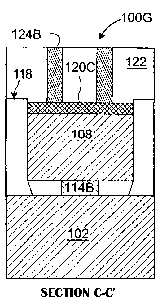
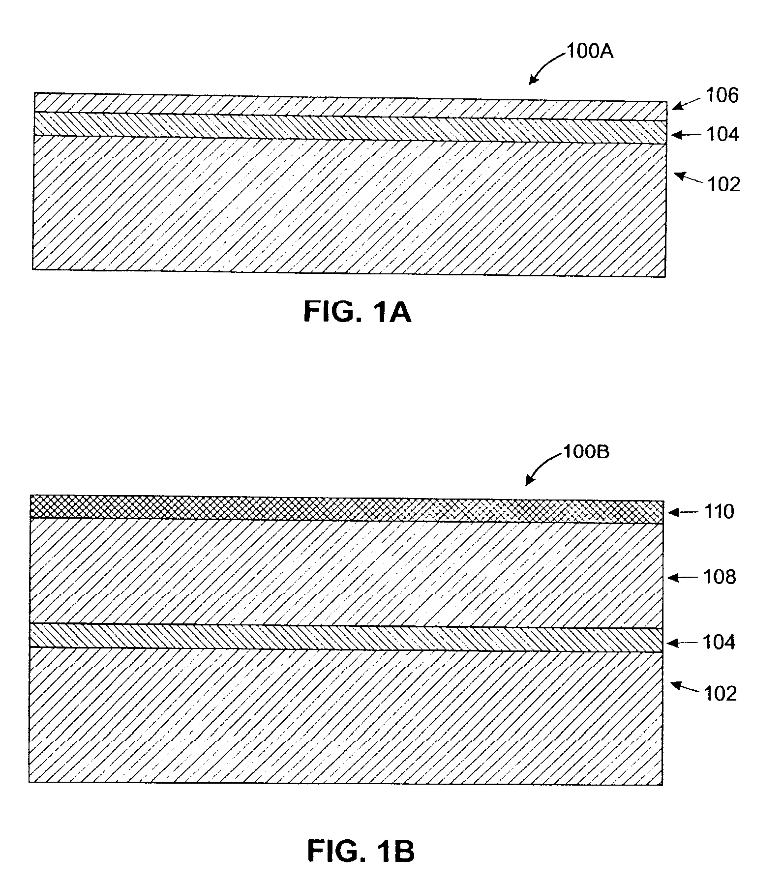
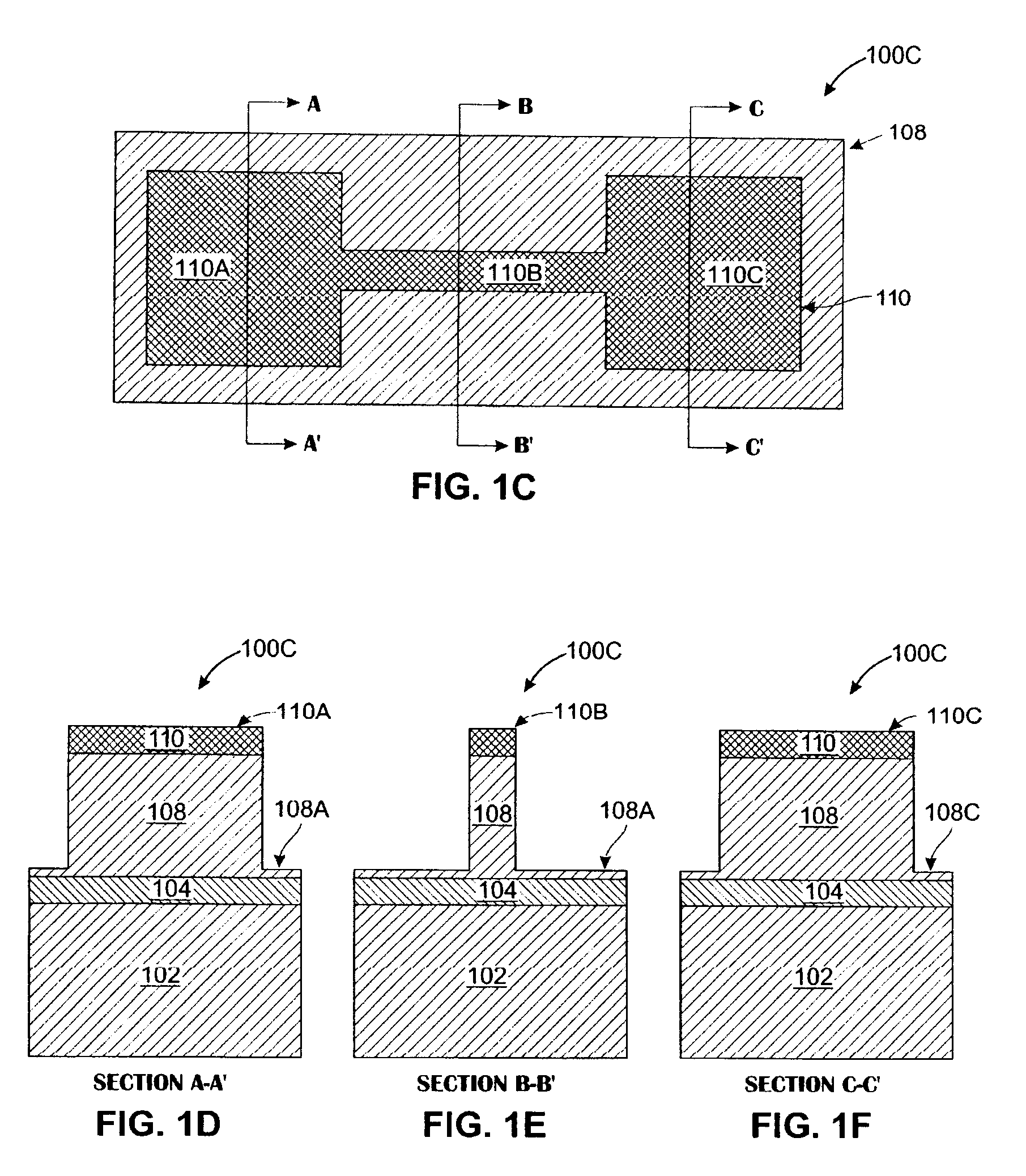
[0063]The present inventive technique creates a “floating beam” eFUSE structure whereby a air gap or air gap is created under a fusible portion of an eFUSE. Typically air fills the space, but it could be just any suitable / convenient gaseous (or vacuum) environment. For example, “undercutting” techniques may be employed whereby a structure is formed atop a buried layer, and that buried layer is removed by selective etching. In-process mechanical support for the floating beam can be provided either by creating a surrounding buttressing support structure or by controlling the selective etch process such that some areas are not fully undercut, leaving supporting “pillars” behind. In either case, a “floating” silicide eFUSE conductor is formed on a silicon beam structure. In its initial state, the eFUSE silicide is highly conductive, exhibiting low electrical resistance (the “unblown state of the eFUSE). When a sufficiently large current is passed through the eFUSE conductor, localized h...


PUM


Abstract

An integrated eFUSE device is formed by forming a silicon “floating beam” on air, whereupon the fusible portion of the eFUSE device resides. This beam extends between two larger, supporting terminal structures. “Undercutting” techniques are employed whereby a structure is formed atop a buried layer, and that buried layer is removed by selective etching. Whereby a “floating” silicide eFUSE conductor is formed on a silicon beam structure. In its initial state, the eFUSE silicide is highly conductive, exhibiting low electrical resistance (the “unblown state of the eFUSE). When a sufficiently large current is passed through the eFUSE conductor, localized heating occurs. This heating causes electromigration of the silicide into the silicon beam (and into surrounding silicon, thereby diffusing the silicide and greatly increasing its electrical resistance. When the current source is removed, the silicide remains permanently in this diffused state, the “blown” state of the eFUSE.

Description

TECHNICAL FIELD[0001]The present invention relates to the formation of structures in semiconductor devices, and more particularly to the formation of electronic fuse (eFUSE) elements on semiconductor devices.BACKGROUND ART[0002]Integrated fuse devices have been employed in semiconductor integrated circuits for many years for a wide variety of purposes. The main purpose of a fuse device is to act a conductive pathway until it is “blown”.[0003]Historically, integrated fuse devices have involved patterned metal conductive links that can be selectively “blown” or cut with a laser beam or by passing a large current through them. This process causes a portion of the link material to vaporize and a portion to melt, in much the same manner as an automotive fuse, but on a much smaller scale. Once blown the fuse changes from a highly conductive state to a highly resistive (i.e., non-conductive) state.[0004]A blown fuse inhibits current from flowing through and represents an open circuit to th...

Claims


Application Information

Patent Timeline
Patent Type & Authority Applications(United States)
IPC IPC(8): H01L29/00H01L21/02
CPCH01L28/20H01L23/5256H01L2924/0002H01L2924/00
Inventor HENSON, WILLIAM K.KIM, DEOK-KEEKOTHANDARAMAN, CHANDRASEKHARANPARK, BYEONGJU
Owner TWITTER INC
Why Eureka
Try Eureka