
Display panel and short circuit detection device thereof
a detection device and display panel technology, applied in the field of detection devices, can solve the problems of long testing time, increased production cost, and inability to quickly and accurately locate defective pixel units, and achieve the effect of quick and accurate identification of defective pixel units
- Summary
- Abstract
- Description
- Claims
- Application Information
AI Technical Summary
Benefits of technology
Problems solved by technology
Method used
Image

Examples
Embodiment Construction
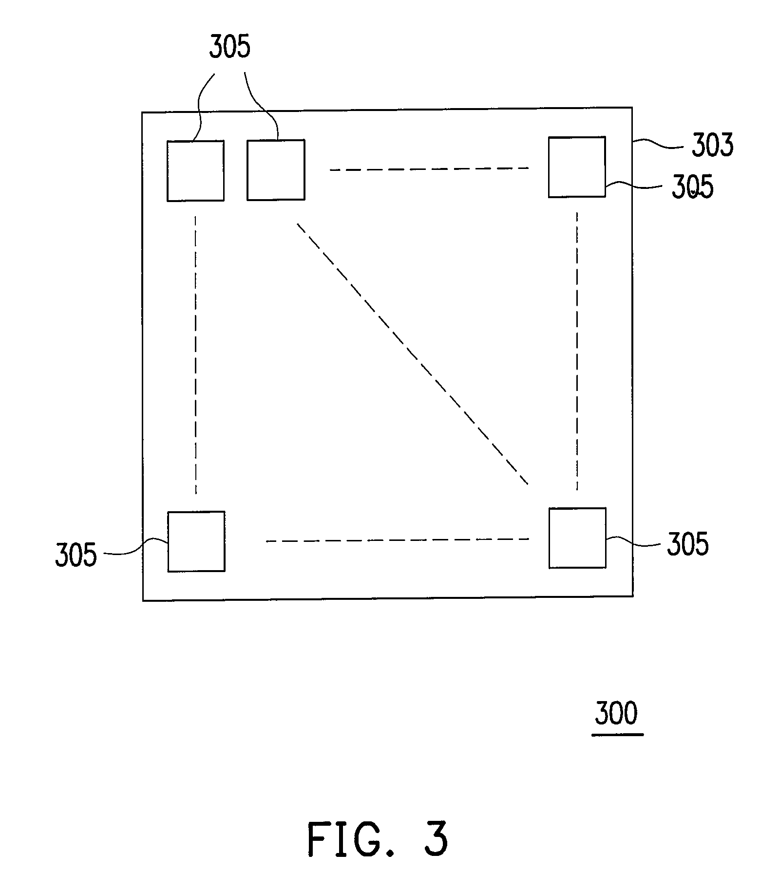
[0023]FIG. 3 illustrates a circuit diagram of a display panel according to one preferred embodiment of the present invention. Referring to FIG. 3, a display panel 300 of the invention includes a substrate 303 and a plurality of display areas 305. The plurality of display areas 305 is arranged as an array and disposed on the substrate 303.
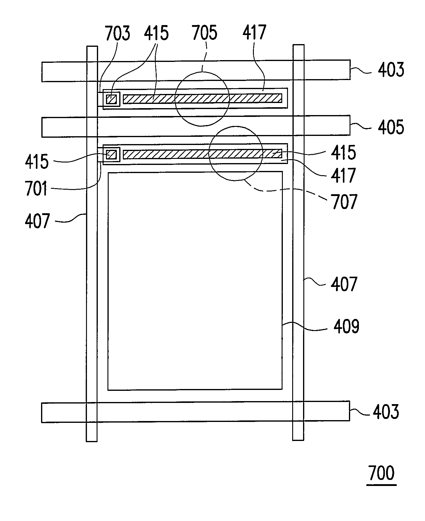
[0024]FIG. 4 illustrates a circuit diagram of a pixel unit according to one preferred embodiment of the invention. The circuit diagram may apply to the display areas 305 of FIG. 3. Referring to FIG. 4, a pixel unit 400 of the invention includes a common voltage electrode 403, a scan electrode 405, a pixel electrode 409, a data electrode 407 and a redundancy electrode 413. It is well-known that the extension direction of the scan electrode 405 may be parallel to the extension direction of the common voltage electrode 403 and substantially perpendicular to the extension direction of the data electrode 407. The extension direction of the scan electrode...
PUM
| Property | Measurement | Unit |
|---|---|---|
| voltage | aaaaa | aaaaa |
| common voltage | aaaaa | aaaaa |
| voltages | aaaaa | aaaaa |
Abstract
Description
Claims
Application Information