Methods and devices for manufacturing of electrical components and laminated structures

a manufacturing method and technology for laminated structures, applied in lamination, weaving, woven fabrics, etc., can solve the problems of high environmental load, unsufficient etching, and high risk of waste management problems of chemical substances employed

Active Publication Date: 2011-04-05
REELTRONICS
View PDF20 Cites 31 Cited by
  • Summary
  • Abstract
  • Description
  • Claims
  • Application Information

AI Technical Summary

Benefits of technology

[0007]It is an object of present invention to provide a method and device facilitating manufacturing of electrical components in a fast and reliable way using a single step.
[0008]It is an other object of present invention to manufacture electrical components on a continuous web or discrete sheets of an inexpensive and easy-to-handle material.
[0009]A further object of present invention is to manufacture electrical components on a continuous web allowing winding to a roll, facilitating storing and shipping and further processing of the electrical components.
[0019]An advantage of the above method, as compared to etching techniques, is that the substrate (i.e. the web or sheet) does not need to become wet. This is particularly advantageous if one desires to use an absorbing material such as paper as carrier material. Furthermore, no residues of the chemicals used are left on any of the processed or unprocessed surfaces.

Problems solved by technology

A drawback inherent in this kind of technique is that the process has to be done in a number of separate steps and thus it is only possible to perform this technique in a continuous process if the feeding rate of the web is low.
An other problem is the possibility of unsufficient etching (when the process is isotropic).
Further, the employed chemical substances give risk to waste management problems and high environmental loads.

Method used


Image

  • Methods and devices for manufacturing of electrical components and laminated structures
  • Methods and devices for manufacturing of electrical components and laminated structures
  • Methods and devices for manufacturing of electrical components and laminated structures

Examples


Embodiment Construction

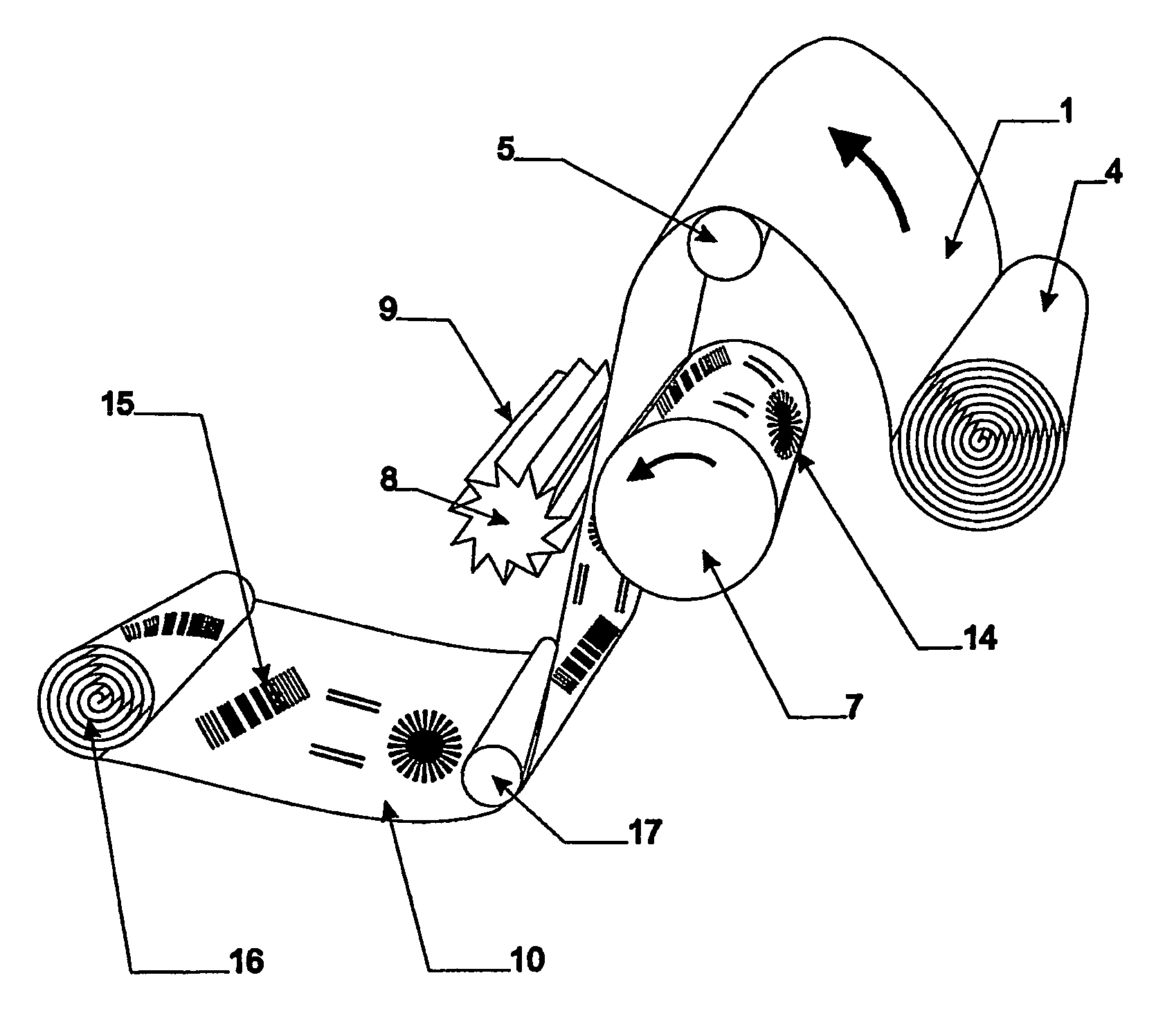
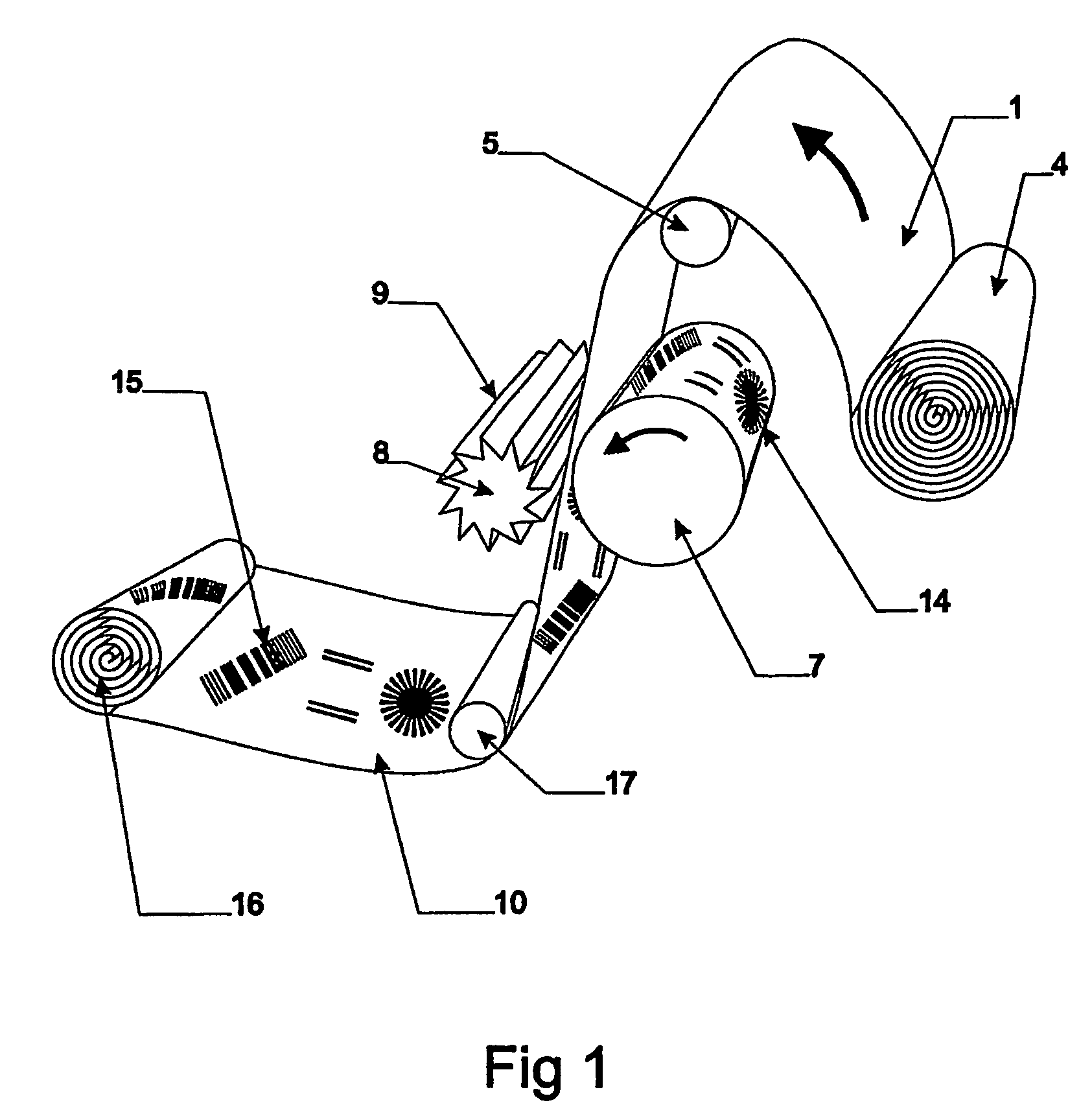
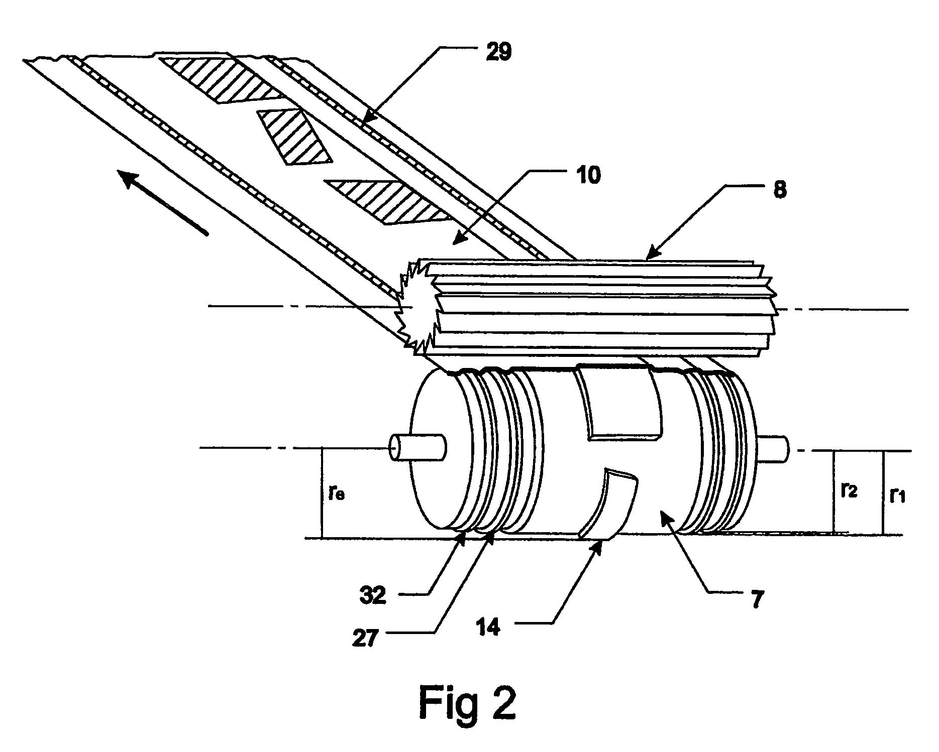
[0032]Referring first to FIGS. 1, 2 and 4 a continuous web 1 consisting of at least one layer 2 of a conducting material, e.g. metal or metal alloy or conducting polymer, and a flexible backing or carrier layer 3 of dielectric material is fed from a supply roll 4, via a support roll 5 to a nip 6. The layer 2 of conducting material is preferably a continuous layer, but it can also be a discontinuous layer consisting of two or more parallel strips oriented in the feeding direction of the web. It is also possible to arrange the layer 2 as discrete areas of conducting material. The backing 3, preferably a plastic (PET) foil or paper, has a more or less consistent thickness t, while the conducting layer 2 may be varying in thickness. The gauges of the different layers are varying, the conducting layer being <1 mm and the backing layer (t) being <1 mm. As will be recognized by a man skilled in the art discrete sheets fed from a supply or storage (not illustrated) may be used instead of sa...


PUM

PropertyMeasurementUnit
flexibleaaaaaaaaaa
conductingaaaaaaaaaa
velocityaaaaaaaaaa

Abstract

A method and device for manufacturing of electrical components on a continuous web or discrete sheets of dielectric material are disclosed. The method includes feeding, from a supply roll of a laminated web or a supply of sheets including at least one unbroken layer of conducting material laminated on a flexible backing layer of dielectrical material, the laminated web or discrete sheets to a nip between a patterned cylinder and a cooperating cylinder, to shape the conducting layer into a repeated pattern of conducting material having ridges and valleys. The method further includes removing, by mechanical machining, conducting material from the thus shaped conducting layer. The removing is performed simultaneously with the step to shape the conducting layer, and by way of the cooperating cylinder, designed as a milling cutter cylinder.

Description

FIELD OF THE INVENTION[0001]Present invention is directed to a method for manufacturing of electrical components on a continuous web of dielectric material or discrete sheets, including the step to feed, from a supply roll of a laminated web or a supply of sheets consisting of at least one layer of conducting material laminated on a flexible backing layer of dielectrical material, said laminated web or discrete sheets to a nip between a patterned cylinder and a cooperating cylinder to shape said conducting layer into a repeated pattern of conducting material having ridges and valleys, and the step to remove by mechanical machining conducting material from said thus shaped metal layer. It is also directed to a device for manufacturing of said electrical components.[0002]More specifically, present invention concerns a method and a device for removing parts of one or more outer layer(-s) from a web or a sheet having a number of layers, at least one layer exhibiting good electrical cond...

Claims


Application Information

Patent Timeline
Patent Type & Authority Patents(United States)
IPC IPC(8): B29C67/20B29C37/02B29C65/00B21D13/00H05K1/00H05K3/04
CPCB32B38/10H05K3/045B29C2043/463B32B2310/0843H05K1/0393Y10T156/1084H05K2203/0143H05K2203/1545Y10T156/12Y10T156/1085H05K2203/0113Y10T442/654Y10T442/656
Inventor NORDLINDER, STAFFANANDERSSON, FREDRIK
Owner REELTRONICS
Why Eureka
Try Eureka