Embedded circuit board and manufacturing method thereof

a technology of embedded circuit boards and manufacturing methods, applied in the direction of conductive pattern formation, association of printed circuit non-printed electric components, chemistry apparatus and processes, etc., can solve the problem of increasing manufacturing costs

a technology of embedded circuit boards and manufacturing methods, applied in the direction of conductive pattern formation, association of printed circuit non-printed electric components, chemistry apparatus and processes, etc., can solve the problem of increasing manufacturing costs

US8552302B2Active Publication Date: 2013-10-08SAMSUNG ELECTRONICS CO LTD

Image

  • Embedded circuit board and manufacturing method thereof
  • Embedded circuit board and manufacturing method thereof
  • Embedded circuit board and manufacturing method thereof

Examples


Embodiment Construction

[0026]Hereinafter, embodiments of the present invention will be described with reference to the accompanying drawings. In the following description, the same elements will be designated by the same reference numerals although they are shown in different drawings. Further, various specific definitions found in the following description are provided only to help general understanding of the present invention, and it is apparent to those skilled in the art that the present invention can be implemented without such definitions.

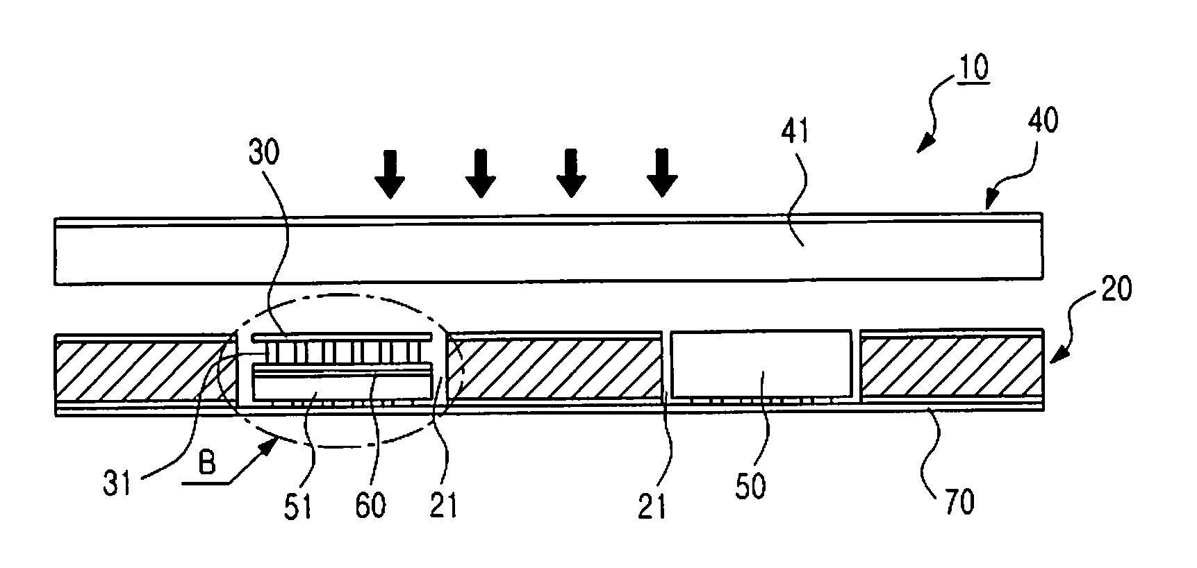
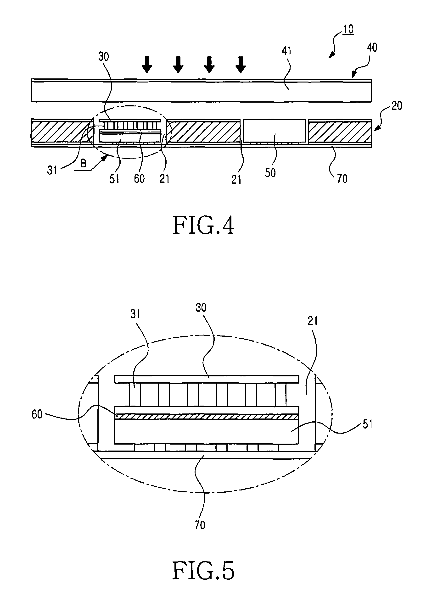
[0027]As shown in FIGS. 4 to 7, an embedded circuit board 10 includes a first Copper Clad Laminate (CCL) 20 formed with a plurality of cavities 21, a second CCL 30, and a RCC 40 coated with resin 41. A plurality of chips 50 and 51 having different thicknesses are embedded in the cavities 21 of the first CCL 20, and a tape 70 is attached to rear surface of the first CCL 20 to support the chips 50 and 51. The second CCL 30 is provided in the cavities 21 to allow the...


PUM

PropertyMeasurementUnit
thicknessesaaaaaaaaaa
adhesiveaaaaaaaaaa
sizeaaaaaaaaaa

Abstract

An embedded circuit board is disclosed including a first copper clad laminate formed with a plurality of cavities and including a plurality of chips having different thicknesses embedded in the cavities, a second copper clad laminate provided in the cavities to allow the first copper clad laminate to level with the chips; and a resin coated copper foil provided on upper surfaces of the first and second copper clad laminates.

Description

PRIORITY[0001]This application claims priority under 35 U.S.C. §119(a) to an application entitled “Embedded Circuit Board And Manufacturing Method Thereof” filed in the Korean Industrial Property Office on Dec. 24, 2009, and assigned Serial No. 10-2009-0131024, the contents of which are incorporated herein by reference.BACKGROUND OF THE INVENTION[0002]1. Field of the Invention[0003]The present invention relates to an embedded circuit board having chips of different thicknesses embedded in a first Copper Clad Laminate (CCL), and a second CCL is provided to allow the chips to level with the first CCL, and a manufacturing method thereof.[0004]2. Description of the Related Art[0005]In general, as electronic products become more highly functional, more lightweight and smaller in size, an increased mounting density is being regarded as an important factor.[0006]With the tendency toward miniaturization, various technologies for mounting a larger number of packages on a board with a limited...

Claims


Application Information

Patent Timeline
08 Oct 2013
Publication
US8552302B2
IPC
H05K1/03
CPC
H05K1/03; H05K1/18; H05K3/10; B32B15/20; H05K7/20; Y10T29/49165
Inventors
PARK, KYUNG-WAN; CHO, SHI-YUN