Supercharge Your Innovation With Domain-Expert AI Agents!

Pixel circuit driving method, light emitting device, and electronic apparatus

a technology of light emitting elements and driving methods, applied in the direction of instruments, computing, electric digital data processing, etc., can solve the problems of insufficient security of compensation operation time, large time needed to make the voltage of both ends, and deviation from a target value or variation among elements, etc., to achieve the effect of suppressing the time for scanning line selection and ensuring the compensation operation tim

Active Publication Date: 2014-02-04
SEIKO EPSON CORP
View PDF14 Cites 4 Cited by
  • Summary
  • Abstract
  • Description
  • Claims
  • Application Information

AI Technical Summary

Benefits of technology

This approach effectively secures time for compensation operations, reduces the speed required for signal line potential supply, and allows for accurate error compensation of threshold voltage and mobility, even if the holding capacitor voltage does not fully reach the threshold voltage, thereby improving the light emitting device's performance and brightness.

Problems solved by technology

The light emitting device has a problem of an error (deviation from a target value or variation among the elements) in characteristics of the driving transistors.
Meanwhile, considerable time is needed to make the voltage of both ends of the holding capacitor approach sufficiently to the threshold voltage of the driving transistor by using the compensation operation.
This causes a problem in that a time for compensation operation is not sufficiently secured.
When the time for the compensation operation is insufficient, it is difficult to make the voltage of both ends of the holding capacitor approach sufficiently to the threshold voltage of the driving transistor.
Accordingly, it is difficult to effectively compensate the error in the threshold voltage of the driving transistor.
On the other hand, when the horizontal scanning period is set to a time that is sufficient to make the voltage of both ends of the holding capacitor approach the threshold voltage of the driving transistor, another problem arises in that an increase (an increase in resolution) in the number of the scanning lines is restricted.

Method used


Image

  • Pixel circuit driving method, light emitting device, and electronic apparatus
  • Pixel circuit driving method, light emitting device, and electronic apparatus
  • Pixel circuit driving method, light emitting device, and electronic apparatus

Examples


modified example 1

1. Modified Example 1

[0078]The conductive types of the transistors (the driving transistor TDR, the selection switch TSL, and the control switch TCR) constituting the pixel circuit U may be optional. For example, as shown in FIG. 11, it may be possible to adopt the pixel circuit U in which the driving transistor TDR and the switches (the selection switch TSL and the control switch TCR) are P-channel types. In the pixel circuit U shown in FIG. 1, the anode of the light emitting element E is connected to the electric supply line 18 (the electric potential VCT), the drain of the driving transistor TDR is connected to the electric supply line 16 (the electric potential VEL[i]), and the source thereof is connected to the cathode of the light emitting element E. Some configurations are the same as the pixel circuit U shown in FIG. 2 in that the holding capacitor C1 is interposed between the gate and the source of the driving transistor TDR, the selection switch TSL is interposed between t...

modified example 2

2. Modified Example 2

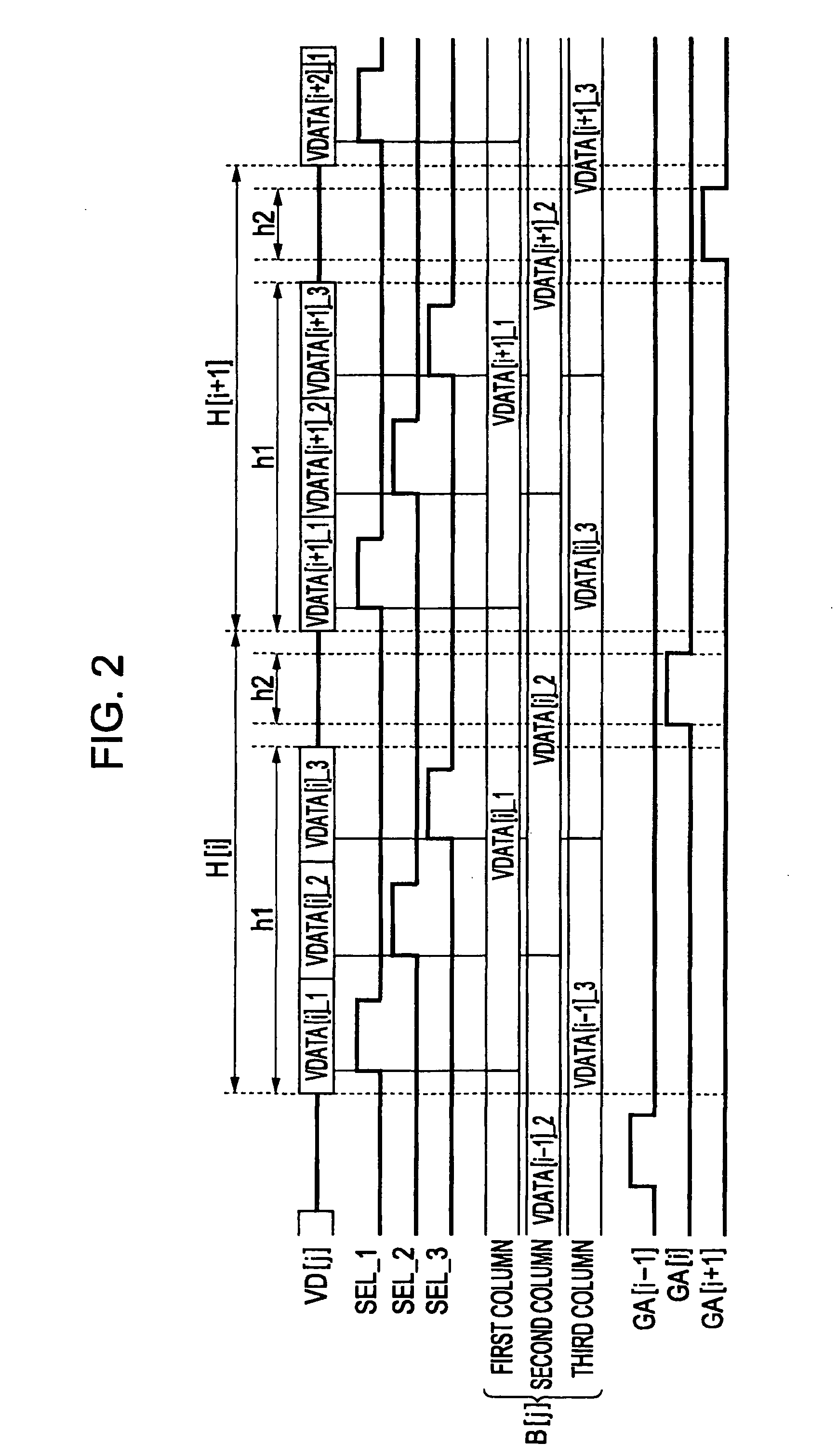
[0079]The number of the unitary periods H used as the reset period PRS and the compensation period PCP may be optional. For example, it may be possible to adopt the configuration in which three or more unitary periods H are used as the compensation period PCP or one unitary period H is used as the compensation period PCP. Even when the compensation period PCP is the one unitary period H, it is possible to achieve a desired effect that can sufficiently secure the time for the reset operation and the first compensation operation according to the embodiment of the invention, compared with the technique disclosed in Japanese Unexamined Patent Application Publication No. 2007-310311 that requires completion of the supply of the gradation potential VDATA, the reset operation, and the first compensation operation within the one unitary period H. In addition, in the above configuration, each of the reset period PRS and the compensation period PCP is started and terminat...

modified example 3

3. Modified Example 3

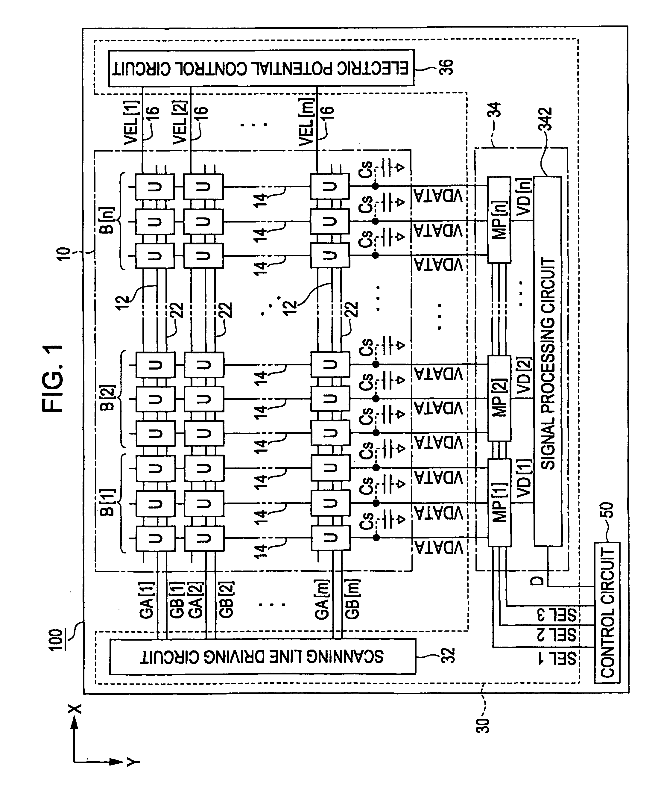
[0080]The number of the signal lines 14 included in the blocks B may be optional. Further, the number of the switches SW constituting the distribution circuits MP may be changed in accordance with the number of the signal lines 14 in the blocks B. In the above-mentioned embodiments, the plurality of signal lines 14 is divided into blocks B when the array of the pixel circuits U of the three colors (red, green, and blue) is set as a unit. However, the method of dividing the plurality of signal lines 14 into the plurality of blocks B may be optional. For example, the plurality of signal lines 14 may be divided into the predetermined number which is determined regardless of the display colors of the pixel circuits U. Furthermore, the configuration in which the plurality of signal lines 14 is divided into the blocks B is not essential. For example, it may be possible to adopt a configuration in which the operations of distributing the gradation potentials VDATA to t...


PUM


Abstract

A method of driving a plurality of pixel circuits. The pixel circuits are disposed corresponding to intersections between a plurality of scanning lines and a plurality of signal lines. Each of the pixel circuits includes: a light emitting element; a driving transistor; a holding capacitor; and a selection switch electrically interconnecting the signal line and the gate of the driving transistor at the time of the selection of the scanning line. The method includes: supplying a gradation potential to each signal line during a first period, selecting the scanning line during a second period, and supplying the gradation potential to the gate of the driving transistor; controlling the driving transistor of each of the pixel circuits to be in an ON state, supplying a reference potential to the gate of the corresponding driving transistor, and executing a first compensation operation and supplying driving current to the light emitting element.

Description

[0001]This application claims priority to Japanese Application No. 2008-226737 filed in Japan on Sep. 4, 2008, the disclosure of which is hereby incorporated by reference in its entirety.BACKGROUND[0002]1. Technical Field[0003]The present invention relates to a technique for driving a light emitting element such as an organic EL (Electroluminescence) element.[0004]2. Related Art[0005]A light emitting device is known in which the driving transistors control the driving current supplied to the light emitting elements. The light emitting device has a problem of an error (deviation from a target value or variation among the elements) in characteristics of the driving transistors. Japanese Unexamined Patent Application Publication No. 2007-310311 discloses a technique that compensates for errors (which may further include an error in an amount of the driving current) in mobility and threshold voltages of the driving transistors by sequentially executing a compensation operation and a rec...

Claims


Application Information

Patent Timeline
Patent Type & Authority Patents(United States)
IPC IPC(8): G09G3/34
CPCG09G3/3233G09G2300/0866G09G2300/0842G09G2300/0819G09G2310/0297
Inventor ISHIGURO, HIDETOYATABE, SATOSHI
Owner SEIKO EPSON CORP
Features
  • R&D
  • Intellectual Property
  • Life Sciences
  • Materials
  • Tech Scout
  • Unparalleled Data Quality
  • Higher Quality Content
  • 60% Fewer Hallucinations
Learn More