Electronic device and method for processing image

a technology of electronic devices and images, applied in image data processing, instruments, television systems, etc., can solve the problems of increasing the total processing time, and achieve the effect of reducing the processing time of the improved image, reducing the processing time, and reducing the accuracy of registration and image fusion

Active Publication Date: 2021-01-12
SAMSUNG ELECTRONICS CO LTD
View PDF27 Cites 0 Cited by
  • Summary
  • Abstract
  • Description
  • Claims
  • Application Information

AI Technical Summary

Benefits of technology

[0004]An image processing solution such as super resolution or High Dynamic Range (HDR) accompanies various processing solutions for several images of the same scene, such that the total processing time may become longer, which may influence the time required to generate a fusion image.
[0005]Accordingly, it is possible to secure the time for some of the processing required for generating the fusion image based on the interval between the time at which a still image is generated and the time at which a next still image is generated.
[0009]Since the image information used for generating an improved image is detected in advance and stored, in various embodiments of the present disclosure, the processing time can be reduced from a point in time at which the event for generating the improved image occurs.
[0010]In various embodiments of the present disclosure, the precision of registration and image fusion performed for generating an improved image can be improved the processing time of the improved image can be reduced, and the image quality level can be improved.

Problems solved by technology

An image processing solution such as super resolution or High Dynamic Range (HDR) accompanies various processing solutions for several images of the same scene, such that the total processing time may become longer, which may influence the time required to generate a fusion image.

Method used


Image

  • Electronic device and method for processing image
  • Electronic device and method for processing image
  • Electronic device and method for processing image

Examples


Embodiment Construction

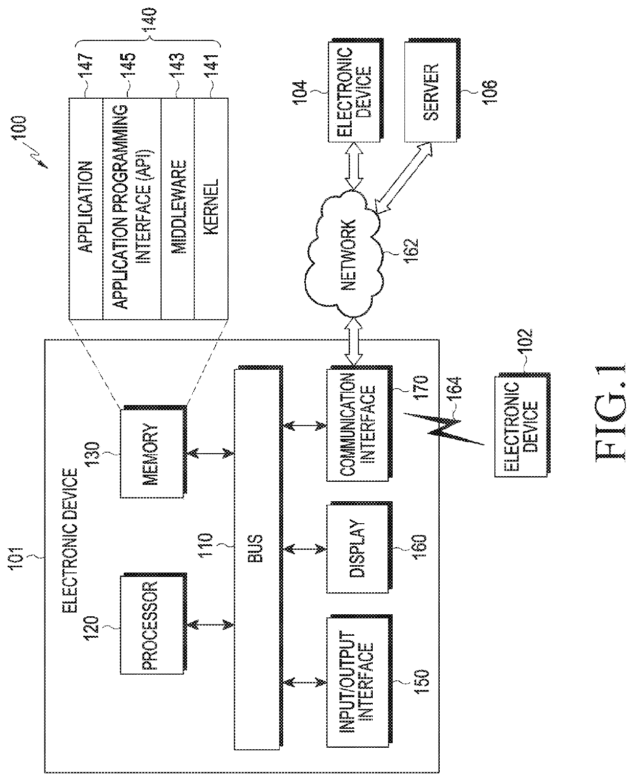
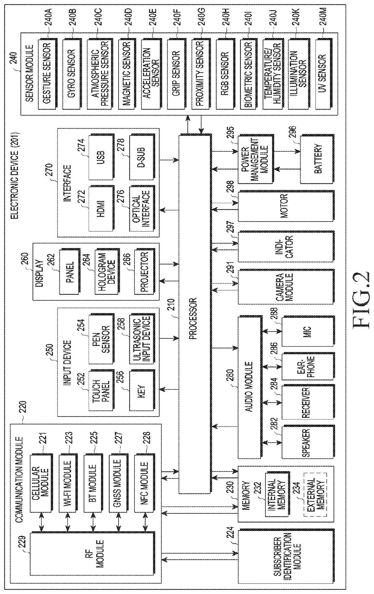
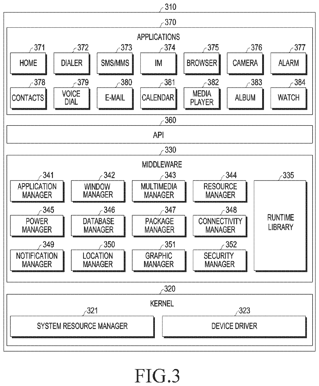
[0020]Hereinafter, various embodiments of the present disclosure will be described with reference to the accompanying drawings. The embodiments and the terms used therein are not intended to limit the technology disclosed herein to specific forms, and should be understood to include various modifications, equivalents, and / or alternatives to the corresponding embodiments. In describing the drawings, similar reference numerals may be used to designate similar constituent elements. A singular expression may include a plural expression unless they are definitely different in a context. In the present disclosure, the expression “A or B”, “at least one of A and / or B”, or “A / B” may include all possible combinations of the items listed. The expression “a first”, “a second”, “the first”, or “the second” used in various embodiments of the present disclosure may modify various components regardless of the order and / or the importance but does not limit the corresponding components. When an elem...


PUM


Abstract

The present invention provides an electronic device and a method for processing an image. A method of the electronic device according to various embodiments can comprise the operations of: obtaining, using an image sensor, a plurality of images including a first image and a second image corresponding to external objects, providing, using the image sensor, at least a part of processed images of the plurality of images as a preview image; detecting image information based on at least the preview image; storing, in a buffer, images including at least the first and second images of the plurality of images; and synthesising, in response to an image capture related input, an image set including at least the first and second images of the images stored in the buffer using the image information so as to create a third image. In addition, the present invention may include other embodiments.

Description

PRIORITY[0001]This application is a National Phase Entry of PCT International Application No. PCT / KR2017 / 002210, which was filed on Feb. 28, 2017, and claims priority to Korean Patent Application No. 10-2016-0038585, which was filed on Mar. 30, 2016, the contents of which are incorporated herein by reference.BACKGROUND1. Field[0002]Various embodiments of the present disclosure relate generally to generating an improved image through various processing processes using a plurality of images.2. Description of the Related Art[0003]In general, a Super Resolution (SR) image is an image which has the maximum resolution and definition that a single image can have, and may be generated by a combination of consecutive low-resolution images obtained during an interval between a time at which a particular still image is generated and a time at which the next still image is generated. Such an SR image may be used for a technique for restoring images of an astronomical telescope and criminal imag...

Claims


Application Information

Patent Timeline
Patent Type & Authority Patents(United States)
IPC IPC(8): H04N5/232H04N5/235H04N5/265H04N5/262G06T3/40G06T7/579G06K9/36G06K9/46
CPCH04N5/232G06T3/4053H04N5/235H04N5/2355H04N5/23232H04N5/23277H04N5/23293H04N5/265H04N23/60H04N23/70H04N23/698H04N23/72H04N23/63H04N23/741H04N23/951H04N23/6845
Inventor MOON, SUNG-HWANMIN, JEONG-HWANPARK, DAE-YUNKIM, MIN-JUNG
Owner SAMSUNG ELECTRONICS CO LTD
Why Eureka
Try Eureka