Photo sensor, display device including the same and driving method thereof

a technology of display device and photo sensor, which is applied in the direction of static indicating device, optical radiation measurement, instruments, etc., can solve the problems of the inability to accurately determine the position of touch, and the inability to accurately determine the presence or absence of touch information, so as to increase the aperture ratio of the display device and increase the accuracy of contact information

Active Publication Date: 2015-12-15
SAMSUNG DISPLAY CO LTD +1
View PDF20 Cites 1 Cited by
  • Summary
  • Abstract
  • Description
  • Claims
  • Application Information

AI Technical Summary

Benefits of technology

[0009]The present invention has been made in an effort to provide a photo sensor having advantages of increasing an aperture ratio of a touch screen display device and increasing accuracy of touch information. Also included are a display device including the same, and a driving method therefor.
[0022]According to the exemplary embodiments of the present invention, it is possible to increase an aperture ratio of the display device including the photo sensor, and also to increase the accuracy of contact information.

Problems solved by technology

In this case, when the sensing signal from the photo current is sufficiently small, touch information such as the presence or absence of touch and a touch position may not be correct.
In either case, when a sensing circuit is complicated or overly large, an aperture ratio of the display device may be undesirably reduced.

Method used


Image

  • Photo sensor, display device including the same and driving method thereof
  • Photo sensor, display device including the same and driving method thereof
  • Photo sensor, display device including the same and driving method thereof

Examples


Embodiment Construction

[0027]The present invention will be described more fully hereinafter with reference to the accompanying drawings, in which exemplary embodiments of the invention are shown. As those skilled in the art would realize, the described embodiments may be modified in various different ways, all without departing from the spirit or scope of the present invention. In the embodiments of the invention that follow, all stated numerical values and ranges are approximate, and can vary.

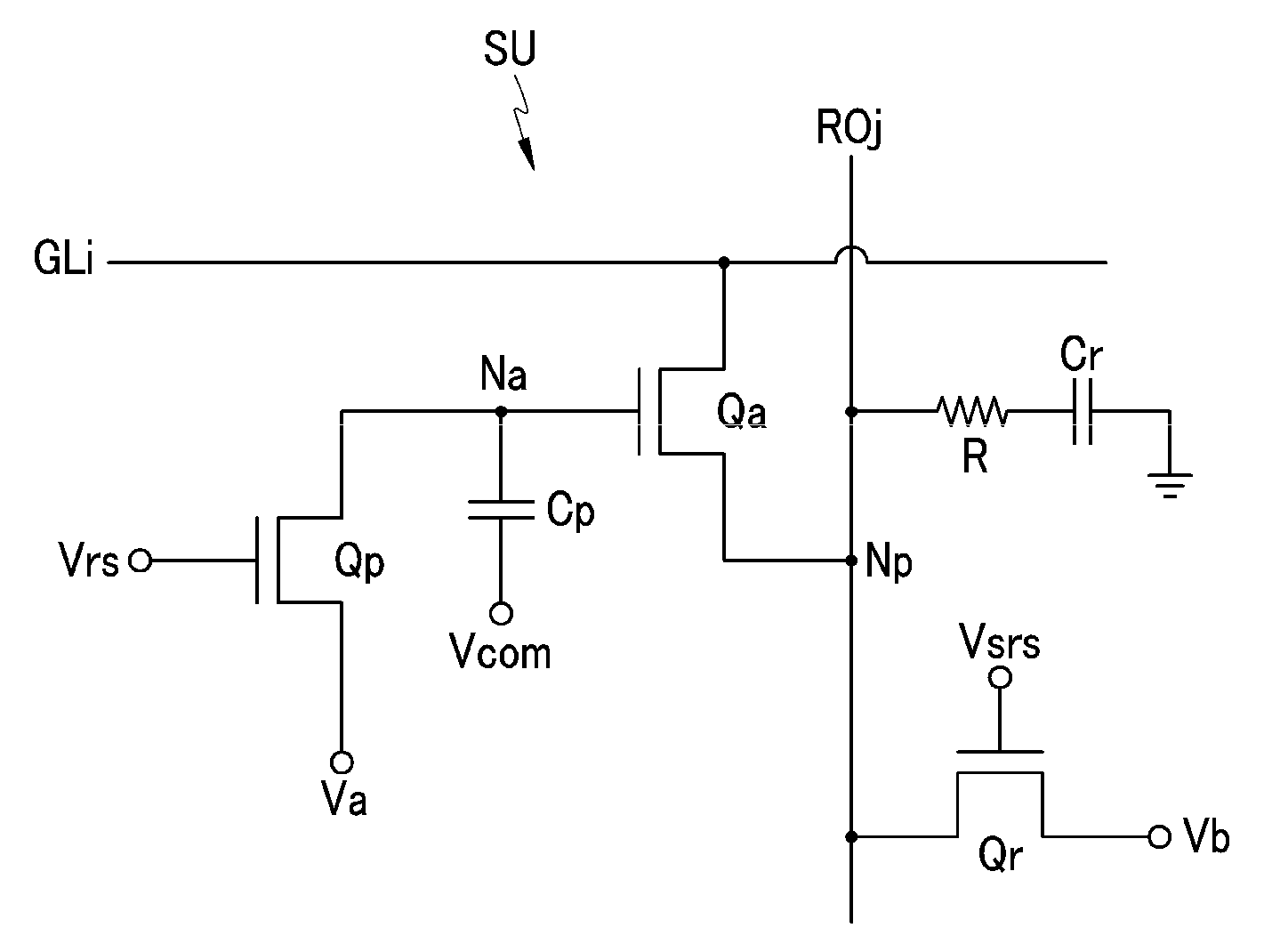
[0028]First, a display device or a touch panel including a photo sensor according to an exemplary embodiment of the present invention will be described with reference to FIG. 1.

[0029]FIG. 1 is a plan view illustrating a display device or a touch panel including a photo sensor according to an exemplary embodiment of the present invention.

[0030]Referring to FIG. 1, a display device or a touch panel including a photo sensor according to an exemplary embodiment of the present invention includes a panel 100 where at leas...


PUM

PropertyMeasurementUnit
voltageaaaaaaaaaa
voltageaaaaaaaaaa
voltageaaaaaaaaaa

Abstract

Provided are a photo sensor, a display device including the same, and a driving method thereof. The photo sensor includes: an amplifying element including an input terminal coupled to a scan line for receiving a scan signal, an output terminal configured to output a sensing signal, and a control terminal connected to a first node; a sensing capacitor connected with the first node; a photosensitive sensing element including a control terminal connected with a terminal of a first control signal, an output terminal connected with the first node, and an input terminal; and a reset element connected with the output terminal of the amplifying element and resetting the output terminal of the amplifying element to second voltage according to a reset control signal.

Description

CROSS-REFERENCE TO RELATED APPLICATION[0001]This application claims priority to, and the benefit of, Korean Patent Application No. 10-2012-0013990 filed in the Korean Intellectual Property Office on Feb. 10, 2012, the entire contents of which are incorporated herein by reference.BACKGROUND OF THE INVENTION[0002](a) Field of the Invention[0003]Embodiments of the invention relate generally to touch screen displays. More specifically, embodiments of the present invention relate to a photo sensor, a display device including the same, and a driving method therefor.[0004](b) Description of the Related Art[0005]The development of touch screen display devices has also entailed development of touch sensors that can be incorporated into such displays. When a user's hand, a touch pen, or the like touches a screen of the display device, the sensor generates an output signal and provides the output signal to the display device. The display device determines touch information such as the presence...

Claims


Application Information

Patent Timeline
Patent Type & Authority Patents(United States)
IPC IPC(8): G01N21/00G01J1/00G09G3/20G01J5/00
CPCG09G3/2092G09G2354/00G09G2360/142G01J11/00G01J5/00
Inventor HAN, SANG YOUNBAE, BYUNG SEONGSONG, JUN HOYANG, SUNG HOONJEON, HO SIK
Owner SAMSUNG DISPLAY CO LTD
Why Eureka
Try Eureka