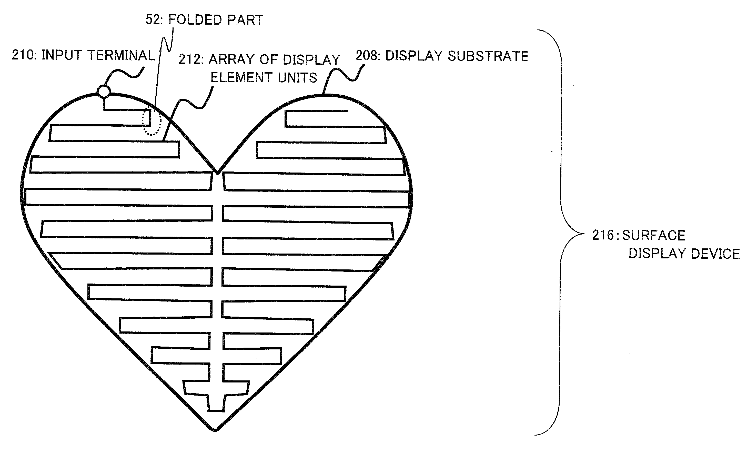
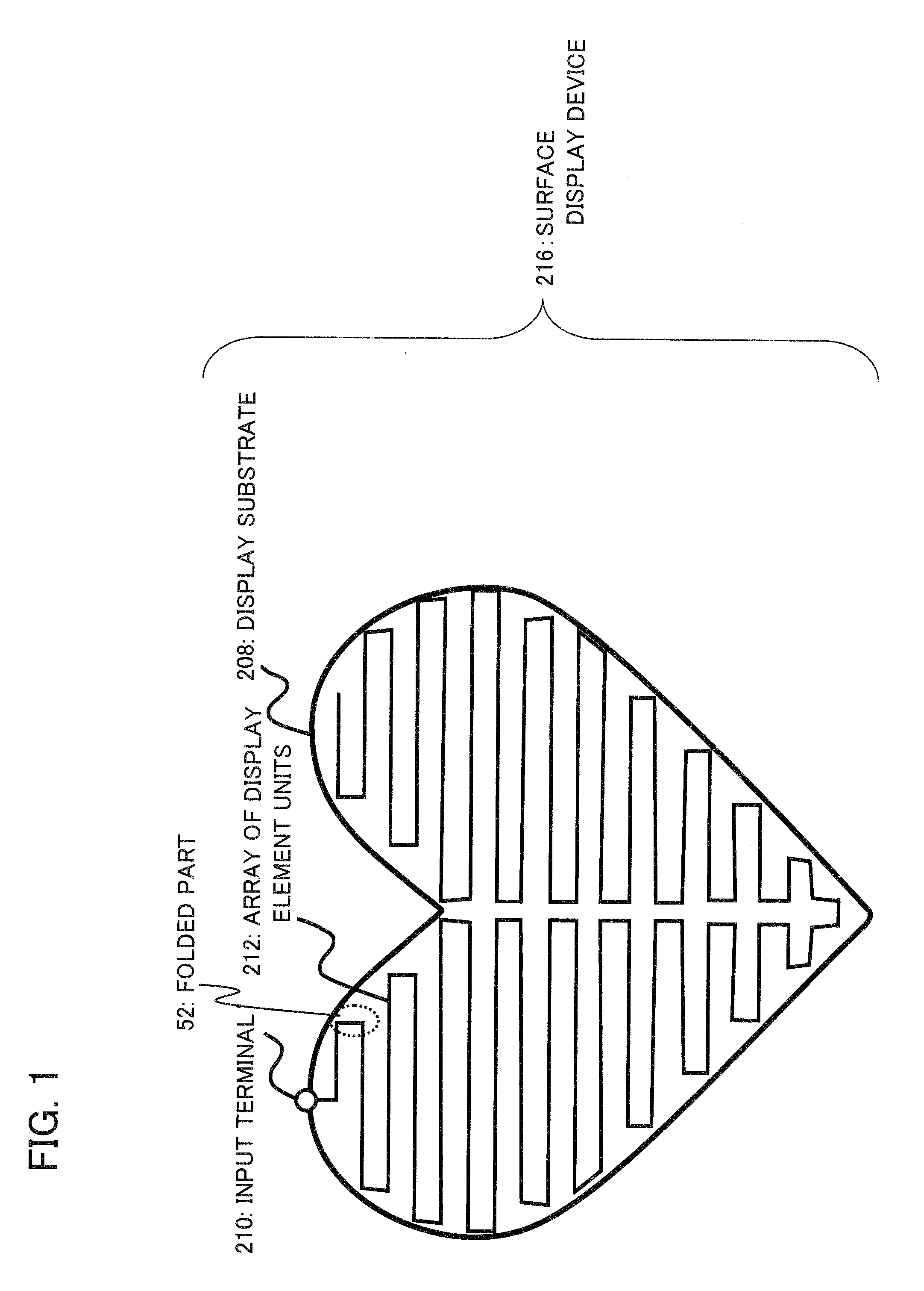
Display device

a display device and surface technology, applied in static indicating devices, non-linear optics, instruments, etc., can solve the problems of limiting the degree of freedom of shape design, the conventional display device cannot afford an arbitrary shape, and placing limitations on the shape freedom of the display device, so as to reduce the number of connection terminals for connection with the circuit driving the display substrate, reduce the number of drivers, and reduce the effect of mask design tim

Active Publication Date: 2008-04-17
BEIHAI HKC OPTOELECTRONICS TECH CO LTD
View PDF11 Cites 102 Cited by
  • Summary
  • Abstract
  • Description
  • Claims
  • Application Information

AI Technical Summary

Benefits of technology

[0056]Still another reason is that, since the display area of the display substrate is constituted by unicursally arranged display element units, it is sufficient that a connection part between the display substrate and the circuit for driving the display substrate is located at an end of the unicursally arranged display element units. Hence, the number of the connection terminals for connection with the circuit driving the display substrate may be reduced, so that there is no necessity of providing the drivers of the TAB type on the outer rim of the display area, or the number of the drivers may be reduced. The bend parts of the TAB are usually linear so that it has been extremely difficult to provide a curved shape of the outer rim of the display substrate.
[0057]The second meritorious effect of the present invention is that mask designing time may be reduced.
[0058]The reason is that there is no necessity of laying out the driver circuit along the curved outer shape of the outer rim. In implementing the present invention, a number of sets of laid-out display element units, with each set being a unit cell, are arrayed along the transverse width of the display area to complete a layout for each row. This process is the same as that of arraying one row of pixels in the conventional process. Heretofore, the driver circuits need to be laid out non-linearly along the outer rim. This operation may be dispensed with and hence the mask designing time may be reduced.
[0059]The third meritorious effect of the present invention is that the frame width of the display device may be decreased.
[0060]The reason is that there is no necessity of providing the driver circuit along the outer rim of the display substrate. That is, the display element units may be arranged up to the outer rim of the display substrate so that the shape of the display substrate will be coincident with the shape of the display area, as a result of which the frame width / length of the display device may be decreased.
[0061]The fourth meritorious effect of the present invention is that the number of connection terminals of the display substrate may be reduced.

Problems solved by technology

The first problem is that the conventional display device cannot afford an arbitrary shape.
That is, the conventional technique allows fabrication of display devices of only a limited range of the non-rectangular shape, but suffers from a highly limited degree of freedom of shape designing.
Since it is necessary to prevent the gate and data wirings from being interrupted, there are placed limitations on the degree of freedom in the shape of the display device.
Depending on the shape of the display device, there is raised a problem that the wirings are partially interrupted such that there may be a non-addressable pixel area in the display device.

Method used


Image

  • Display device
  • Display device
  • Display device

Examples


example 1

[0153]In the present example, a TFT substrate (Thin Film Transistor) substrate is prepared, using the polysilicon process technique, and an active matrix liquid crystal display device was fabricated using this substrate. The sell-known low-temperature polysilicon TFT-LCD fabrication technique was used as fabrication process. The detailed process for fabrication is stated in “Illustrated Low-Temperature poly-Si TFT-LCD Fabrication Process, 2005-issue, published by E-Express Co. Ltd.

[0154]Using the technique for low-temperature fabrication of polysilicon TFT-LCD, a TFT pixel switch of a planar configuration, a TFT of a scanning circuit and an electrode of the storage capacitor, were prepared to form a TFT substrate.

[0155]The TFT that forms a circuit on a display substrate was prepared as a TFT of the same process. That is, the process is such as enables the operation of a TFT in need of a high voltage.

[0156]A patterned pillar of 4 μm was prepared on this TFT substrate for use as a spa...

example 2

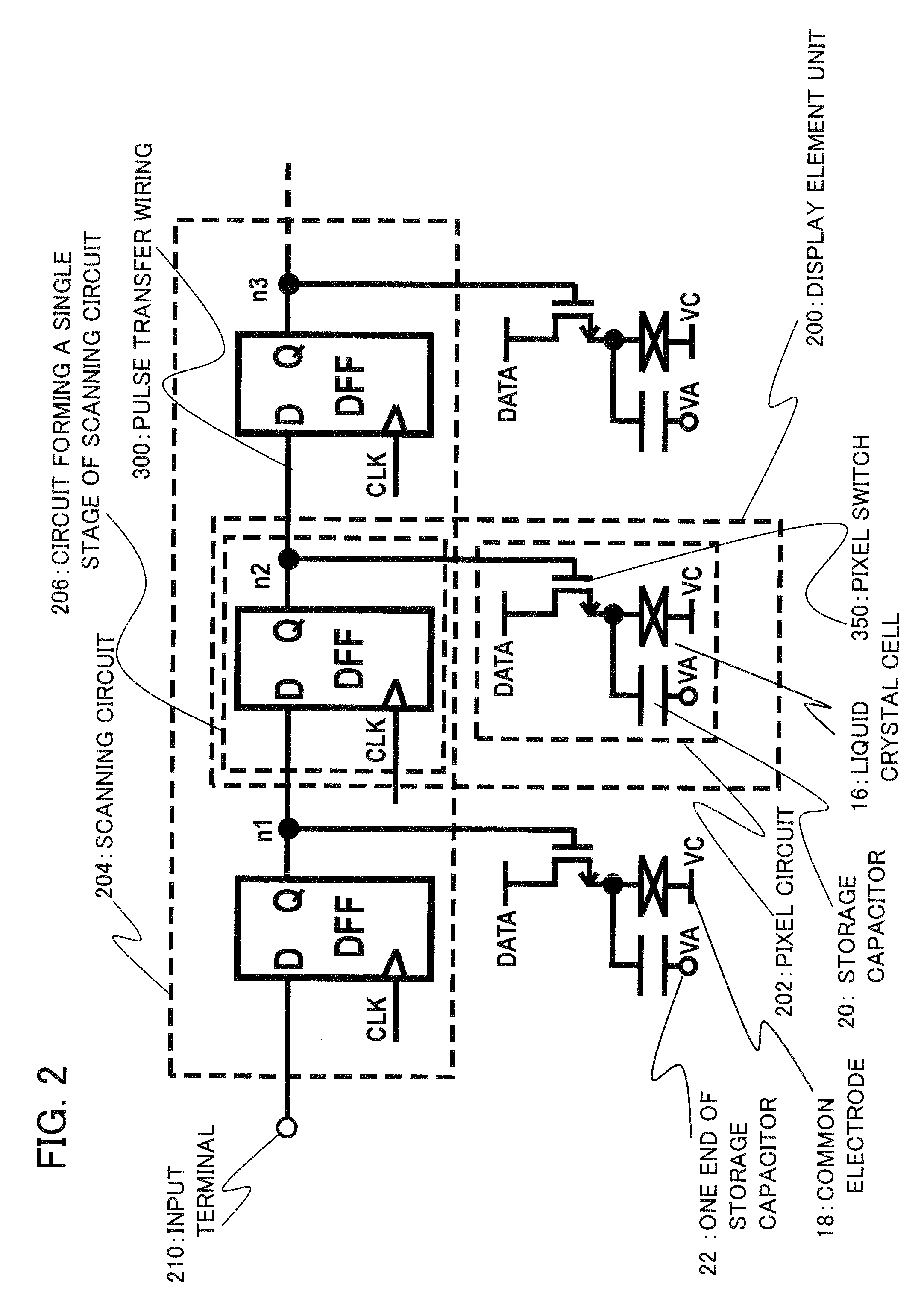
[0180]In the case of the example 1 of FIGS. 11A and 11B, 21 transistors for each pixel and a two-phase clock signal, namely a clock signal for driving the scanning circuit and the inverted clock signal, are required.

[0181]The present example, which will now be described, has been devised by the present inventor to reduce the number of the transistors and the number of the clock signals.

[0182]FIG. 13 shows the configuration of the scanning circuit and the pixel circuit of the present example. In FIG. 13, a display device (200) is made up of a circuit (206), forming a stage of the scanning circuit, and a scanning circuit (202), connected to an output node of the circuit (206). This circuit (206), forming a stage of the scanning circuit, is made up of a sole inverter circuit and a sole switching transistor. Switching transistors 214a and 214c are of the n-type and switching transistors 214b and 214d are of the p-type. That is, the first-stage switching transistor 214a, second-stage swi...

example 3

[0206]An example 3 of the present invention will now be described. Referring to FIGS. 15A and 15B, the scanning circuit (204) of the present example includes a clocked inverter (56) per stage of the scanning circuit.

[0207]A sole pixel switch (350) is connected to output nodes n1, n2, n3, . . . of the circuit (206) that constitutes a stage of the scanning circuit. The pixel switch, connected to the output node 1, is of the p-type, that connected to the output node n2 is of the n-type and that connected to the output node n3 is of the p-type, and so forth. That is, the pixel switches connected to the odd and the even stages of the scanning circuit are of the p-type and the n-type, respectively.

[0208]Thus, a display device may be implemented using five transistors per pixel. The clock signal that drives the scanning circuit is CLK and its inversion XCLK.

[0209]The operation of the scanning circuit and the pixel circuit, constructed as described above, is now described. FIG. 16 depicts a...


PUM


Abstract

Disclosed is a display device for use of a surface display of an arbitrary shape, including a plural number of display element units, each made up of a circuit that forms a single stage of a scanning circuit and a pixel circuit connected to an output of the scanning circuit, are arranged in a unicursal fashion on a display substrate.

Description

REFERENCE TO RELATED APPLICATION[0001]The present application is claiming the priority of the earlier Japanese patent application No. 2006-280234 filed on Oct. 13, 2006, the entire disclosure thereof being incorporated herein by reference thereto.FIELD OF THE INVENTION[0002]This invention relates to a display device. More particularly, this invention relates to a surface display device, such as a liquid crystal display or an EL (electroluminescence) display, being able to have a display surface shape other than a rectangular surface shape.BACKGROUND OF THE INVENTION[0003]In an active matrix liquid crystal display device, a plurality of pixels are arranged in rows and columns, that is, in a matrix array. Each row of the matrix of pixels shares a gate wiring connected to the gate electrodes of thin-film transistors (TFTs). Each column of the matrix of pixels shares a data wiring supplied with a data signal. The signal on the gate wiring on / off controls the thin-film transistors, such ...

Claims


Application Information

Patent Timeline
Patent Type & Authority Applications(United States)
IPC IPC(8): G09G3/36
CPCG09G3/18G02F1/136286G02F1/134336G09G2310/0267G09G2300/0426G09G3/3648G09G2300/043G09G2310/0232G09G2320/0214
Inventor HAGA, HIROSHIASADA, HIDEKIKANEKO, SETSUO
Owner BEIHAI HKC OPTOELECTRONICS TECH CO LTD
Why Eureka
Try Eureka