Pixel structure of active matrix organic light emitting display and fabrication method thereof

a technology of organic light emitting display and active matrix, which is applied in the manufacture of electrode systems, electric discharge tubes/lamps, discharge tubes luminescnet screens, etc., can solve the problems of reducing the longevity and the efficiency of the passive driving device, and damaging so as to minimize the damage to the organic emitting layer

Inactive Publication Date: 2008-05-22
AU OPTRONICS CORP
View PDF8 Cites 106 Cited by
  • Summary
  • Abstract
  • Description
  • Claims
  • Application Information

AI Technical Summary

Benefits of technology

[0014]The present invention is related to a fabrication method for the pixel structure of active matrix organic light emitting diode (AMOLED) display to minimize the damage to the organic emitting layer caused by the sputtering process.
[0015]The present invention is further related to a pixel structure of AMOLED display having a better light transmission rate and aperture ratio.
[0037]The fabrication method for the pixel structure of AMOLED display of the present invention begins with the formation of OLED followed by the formation of TFT, and the pixel structure is bottom-emitting type. As a result, the light emitted by the OLED will not pass through the TFT, thus greatly increasing the aperture ratio. Furthermore, since the transparent electrode, the organic emitting layer and the reflective electrode are fabricated sequentially, the organic emitting layer is prevented from being damaged by the formation of the transparent electrode while retaining the light transmission rate of OLED.

Problems solved by technology

Nevertheless, the luminescent efficiency and the longevity of the passive driving device drastically decline as the size and the resolution of the display increases.
As a result, the formation of the anode 136 often damages the organic emitting layer 134.

Method used


Image

  • Pixel structure of active matrix organic light emitting display and fabrication method thereof
  • Pixel structure of active matrix organic light emitting display and fabrication method thereof
  • Pixel structure of active matrix organic light emitting display and fabrication method thereof

Examples


Embodiment Construction

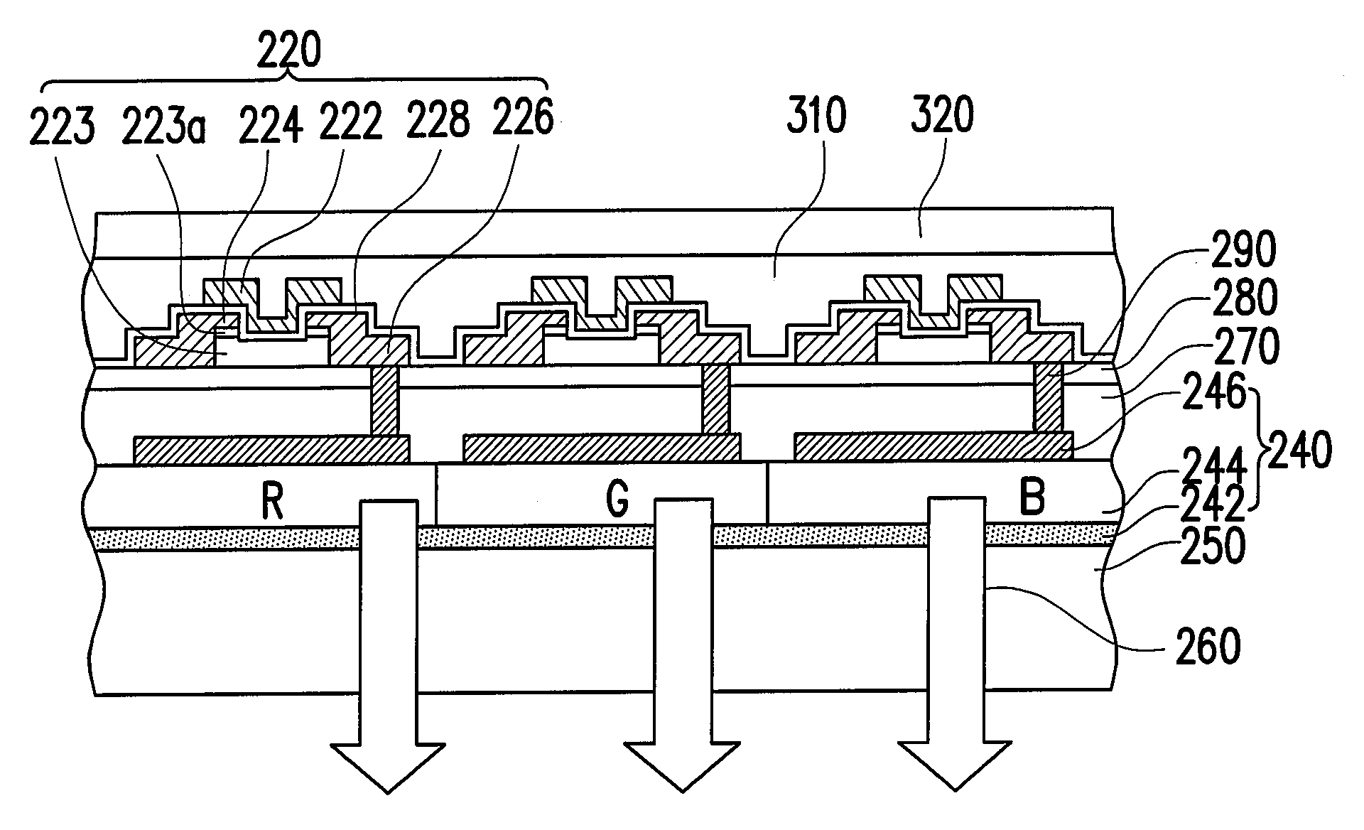
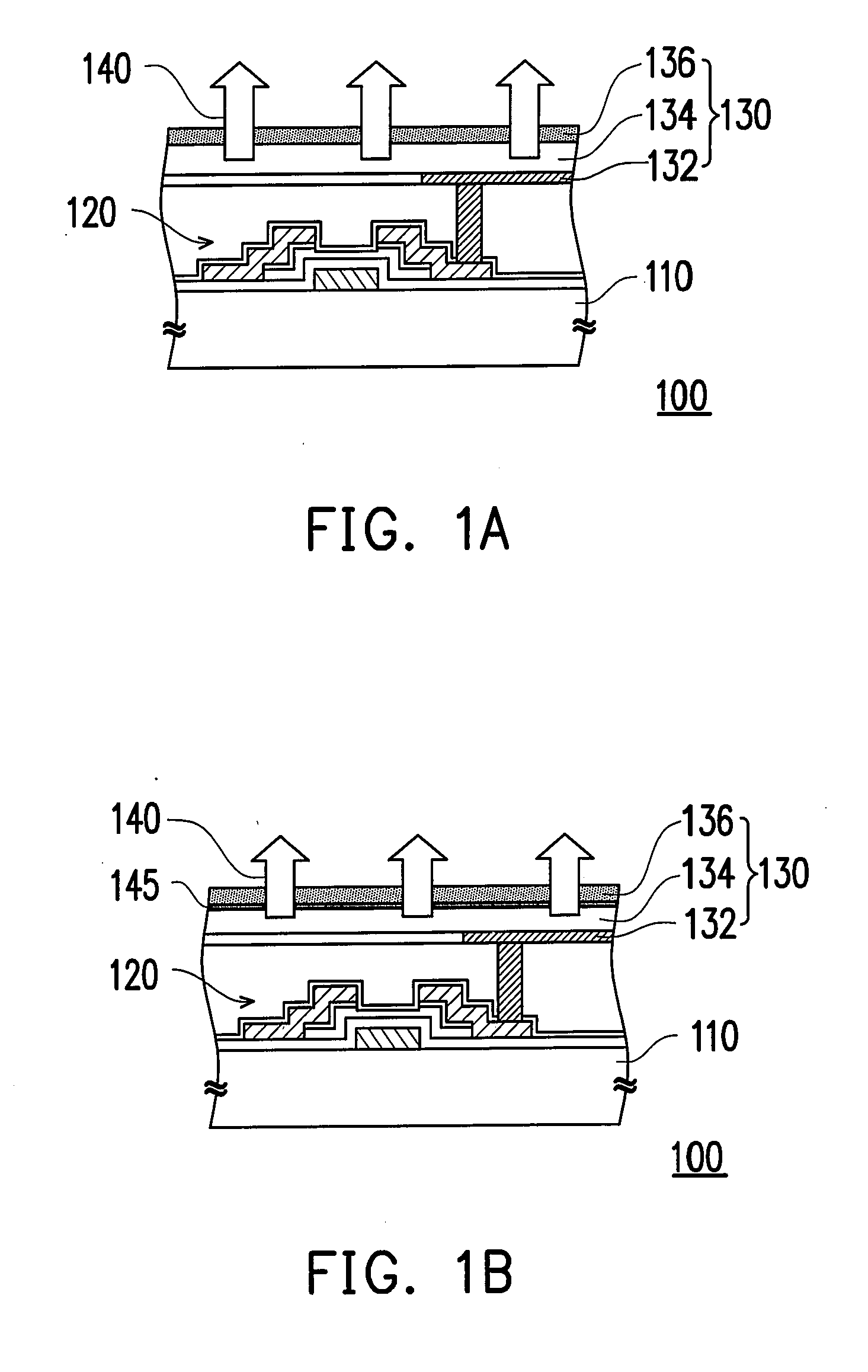
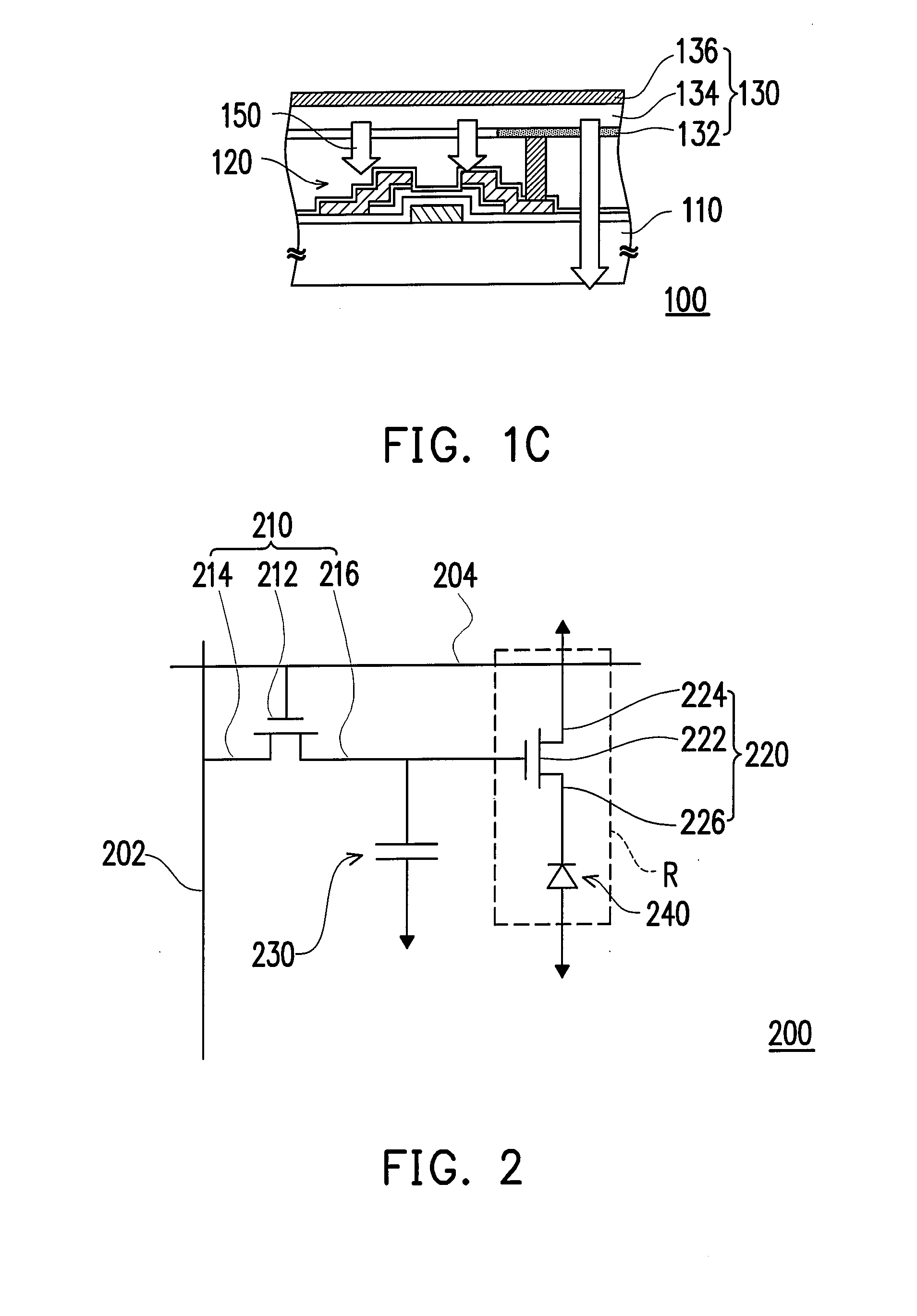
[0043]To solve the problems encountered by the conventional technology, the present invention provides a fabrication method for the pixel structure of AMOLED display and the pixel structure of AMOLED display. This fabrication method begins with the formation of OLED first, followed by the formation of TFT. The pixel structure disclosed by the present invention is similar to the structure of the thin film transistor array on color filter (TFT-array on color filter, TOC or AOC) used in liquid crystal display (LCD).

[0044]Generally, the channel of TFT is fabricated using amorphous silicon or polysilicon, wherein polysilicon demonstrates better electron mobility. Therefore, TFT utilizing a polysilicon channel provides a better device performance. Nonetheless, the temperature for fabricating polysilicon is usually above 300° C. Since OLED cannot withstand the high temperature for fabricating polysilicon channel layer, the structure of OLED is damaged as a result of the formation of the po...


PUM


Abstract

A pixel structure of active matrix organic light emitting display and method for fabricating the same are provided. In the method, a transparent electrode, an organic light emitting diode, and a reflective electrode are formed on a substrate. Subsequently, at least one switching thin film transistor, at least one driving thin film transistor, a scan line, a data line, and a storage capacitor are formed over the substrate.

Description

CROSS-REFERENCE TO RELATED APPLICATION[0001]This application claims the priority benefit of Taiwan application serial no. 95142537, filed Nov. 17, 2006. All disclosure of the Taiwan application is incorporated herein by reference.BACKGROUND OF THE INVENTION[0002]1. Field of the Invention[0003]The present invention relates to an active matrix organic light emitting display (AMOLED) and more particularly, a thin film transistor disposed on the light emitting diode (LED) of the pixel structure of active matrix organic light emitting display and fabrication method thereof.[0004]2. Description of Related Art[0005]An organic light emitting diode is a semiconductor device that transforms electrical energy to light energy. It is known for its high luminescent efficiency, wide range of viewing angle, simple manufacturing process, low manufacturing cost, high response speed, wide operating temperature range and full color. These advantages of organic light emitting diode (OLED) overlap with m...

Claims


Application Information

Patent Timeline
Patent Type & Authority Applications(United States)
IPC IPC(8): H01J1/62H01J9/00
CPCH01L27/322H01L27/3244H01L27/1255H01L51/56H01L27/3258H01L27/326
Inventor HSU, SHIEN-CHILIN, CHIN-YUANYU, WEI-SHENGLU, YI-JUNHSU, SHU-CHING
Owner AU OPTRONICS CORP
Why Eureka
Try Eureka