LCD panel and pixel structure thereof

a technology of liquid crystal display and pixel structure, applied in the direction of non-linear optics, static indicating devices, instruments, etc., can solve the problems of increased costs and achieve the effect of low color washout design requirements

Active Publication Date: 2017-04-11
TCL CHINA STAR OPTOELECTRONICS TECH CO LTD
View PDF8 Cites 0 Cited by
  • Summary
  • Abstract
  • Description
  • Claims
  • Application Information

AI Technical Summary

Benefits of technology

[0016]The discharge of the sub-pixel electrode could be realized by the pixel structure of the liquid crystal display panel provided by the present invention, without increasing the scanning lines, thus to achieve low color washout design requirements, moreover, the pixel structure could be compatible with forward scan and reverse scan that is suitable for a wide range of applications.

Problems solved by technology

However, twice number of such chip on films (COF) that must be used in according to this method results increased costs.

Method used


Image

  • LCD panel and pixel structure thereof
  • LCD panel and pixel structure thereof
  • LCD panel and pixel structure thereof

Examples


Embodiment Construction

[0022]Technical solutions of embodiments of the present invention will be clearly and completely described below referring to the drawings. Obviously, the embodiments will be described are only part but not all of the embodiments of the present invention. All other embodiments obtained by no creative work of ordinary skills according to the embodiments of the present invention are within the scope of the present invention.

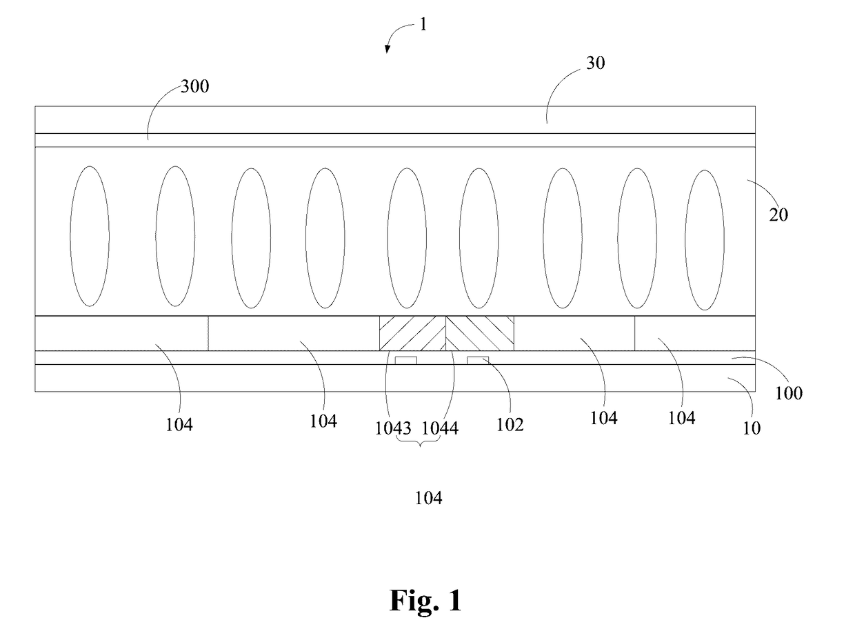
[0023]Please refer to FIG. 1, a liquid crystal display (LCD) panel 1 includes an array substrate 10, a liquid crystal layer 20 and a color filter substrate 30. Wherein the array substrate 10 is oppositely disposed with the color filter substrate 30, and the liquid crystal layer 20 is interposed between the array substrate 10 and the color filter substrate 30.

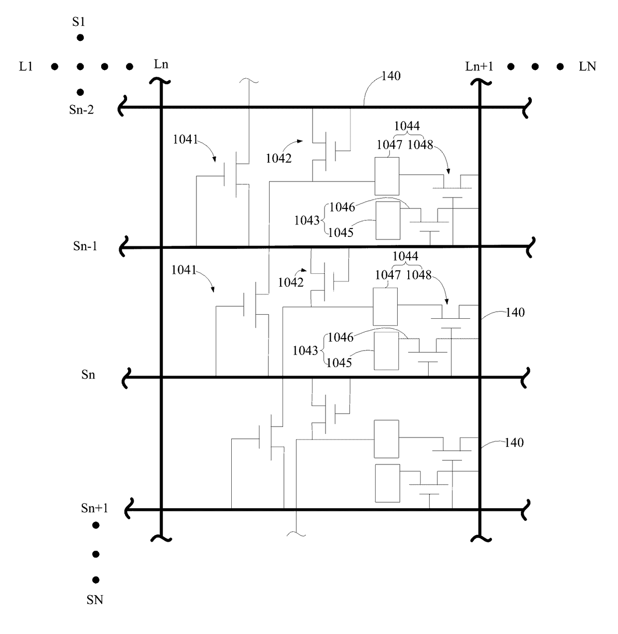
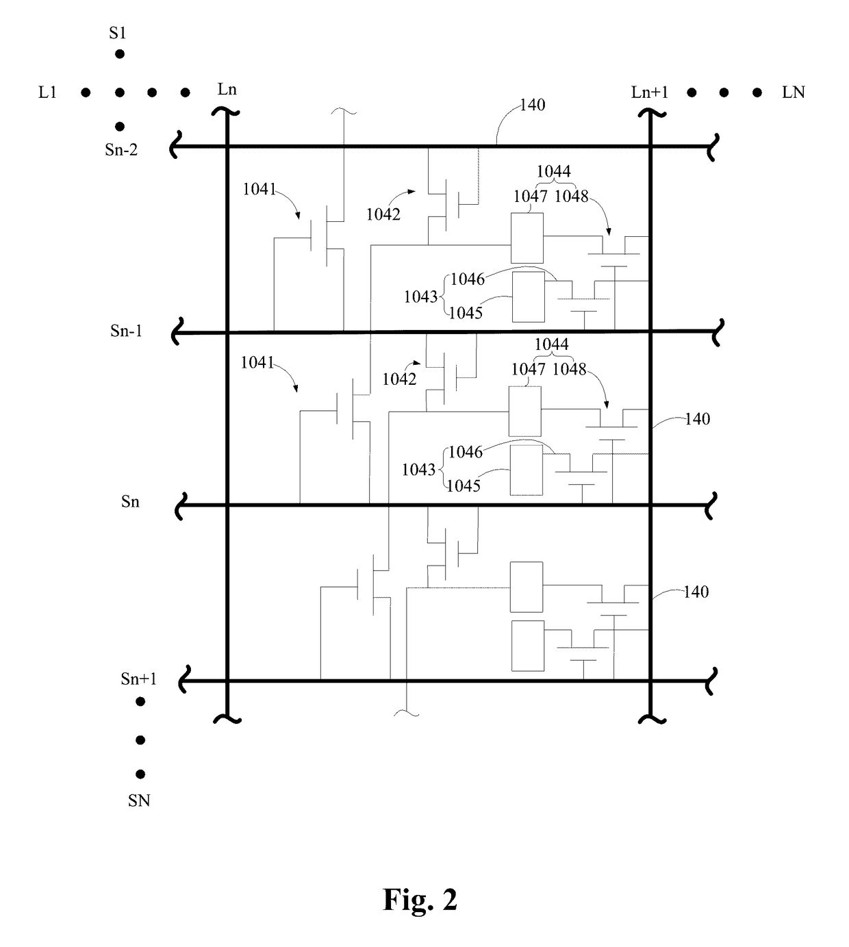
[0024]The array substrate 10 includes an insulating layer 100, a storage capacitor electrode 102 and a plurality of pixel cells 104 having said pixel structure disposed on the insulating layer 100 to display di...


PUM

PropertyMeasurementUnit
colorsaaaaaaaaaa
areaaaaaaaaaaa

Abstract

The present invention provides a pixel structure including a plurality of pixel cells arranged in a matrix. The pixel cells are defined by a plurality of scan lines and data lines that being mutually intersected. Each pixel cell includes a first discharge control switch, a second discharge control switch, a main pixel area and a sub-pixel region is disposed adjacent the latter. The main pixel area includes a main pixel electrode and a main charge control switch. The sub-pixel area includes a sub-pixel electrode and a sub-charge control switch. The main pixel electrode receives display signals by the main charge control switch. The sub-pixel electrode receives display signals by the sub-charge control switch. The scan line transmitting scan signals of its present pixel cell and the sub-pixel electrode of the above pixel cell are connected by said first discharge control switch.

Description

FIELD OF THE INVENTION[0001]The present invention relates to LCD (liquid crystal display) panels and pixel structures thereof.BACKGROUND OF THE INVENTION[0002]Pixel structure of a current type of LCD panel with low color washout might be implemented by increasing scan lines to respectively control different regions of a same pixel. However, twice number of such chip on films (COF) that must be used in according to this method results increased costs.[0003]Therefore, it's desirable to provide a LCD panels and pixel structure thereof, which can overcome the above-described problem.SUMMARY OF THE INVENTION[0004]To solve the above technical problem, embodiments of the present invention provide a pixel structure, which comprises a plurality of pixel cells arranged in a matrix. The pixel cells are defined by a plurality of scan lines and data lines that are mutually intersected. Each pixel cell comprises a first discharge control switch, a second discharge control switch, a main pixel are...

Claims


Application Information

Patent Timeline
Patent Type & Authority Patents(United States)
IPC IPC(8): G09G3/36G02F1/1362G02F1/1333G02F1/1368G02F1/1335G02F1/133G02F1/1343
CPCG09G3/3677G02F1/1368G02F1/13306G02F1/13624G02F1/133345G02F1/133514G02F1/134336G02F1/136286G09G3/3688G02F2001/134345G02F2201/121G02F2201/123G09G2300/0426G09G2300/0814G09G2310/0251G09G2320/0242G02F1/134345
Inventor HUANG, SHISHUAICHANG, TIEN-HAO
Owner TCL CHINA STAR OPTOELECTRONICS TECH CO LTD
Why Eureka
Try Eureka