Touch-panel-equipped display device
a display device and touch panel technology, applied in the field of touch panel-equipped display devices, can solve the problems of moire occurrence and the inability to solve the deterioration of display quality due to moire in some cases, and achieve the effect of suppressing the occurrence of moir
- Summary
- Abstract
- Description
- Claims
- Application Information
AI Technical Summary
Benefits of technology
Problems solved by technology
Method used
Image


Examples
embodiment 1
[Configuration of Touch-Panel-Equipped Display Device]
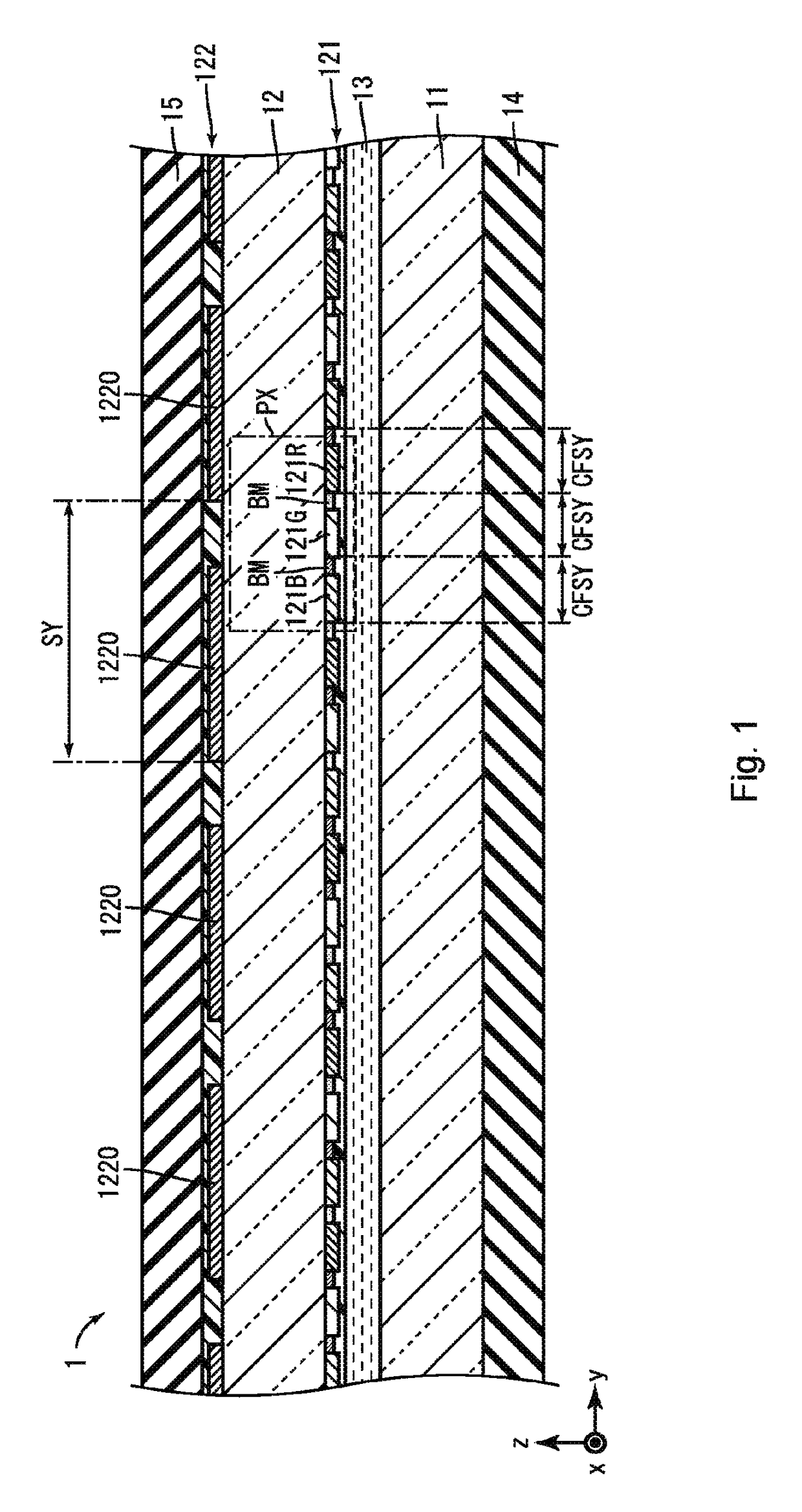
[0041]FIG. 1 is a cross-sectional view schematically illustrating a configuration of a touch-panel-equipped display device 1 according to Embodiment 1 of the present invention. The touch-panel-equipped display device 1 includes: an active matrix substrate 11 and a color filter substrate 12 that are arranged so as to be opposed to each other; a liquid crystal layer 13 sealed between these substrates; and polarizing plates 14 and 15.
[0042]For convenience of explanation, the x direction (first direction), the y direction (second direction), and the z direction are set as illustrated in FIG. 1. The x direction, the y direction, and the z direction intersect at right angles. The direction parallel with the thickness direction of the touch-panel-equipped display device 1 is defined as the z direction.
[0043]On the active matrix substrate 11, a plurality of pixel electrodes are formed, though a detailed configuration thereof is not shown...
embodiment 2
[Embodiment 2]
[0085]A touch-panel-equipped display device according to Embodiment 2 of the present invention is identical to the touch-panel-equipped display device 1 except that a sensor pattern layer 222 is provided in place of the sensor pattern layer 122.
[0086]FIG. 10 is a plan view illustrating the configuration of the sensor pattern layer 222. The sensor pattern layer 222, as is the case with the sensor pattern layer 122, includes a plurality of electrodes 2220 arranged along the y direction at a sensor interval SY. Each of the electrodes 2220 is formed so as to have a bias angle θ between the same and the x direction.
[0087]Each of the electrodes 2220 is turned every ½ of a predetermined cycle SPN in the x direction in such a manner that the angle formed between the same and the x direction is reversed.
[0088]According to the present embodiment, the electrodes 2220 can be formed approximately in a linear form parallel to the x direction over a long section, which increases the ...
PUM
| Property | Measurement | Unit |
|---|---|---|
| bias angle | aaaaa | aaaaa |
| aspect ratio | aaaaa | aaaaa |
| bias angle | aaaaa | aaaaa |
Abstract
Description
Claims
Application Information
 - R&D
- Intellectual Property
- Life Sciences
- Materials
- Tech Scout
- Unparalleled Data Quality
- Higher Quality Content
- 60% Fewer Hallucinations
Browse by: Latest US Patents, China's latest patents, Technical Efficacy Thesaurus, Application Domain, Technology Topic, Popular Technical Reports.
© 2025 PatSnap. All rights reserved.Legal|Privacy policy|Modern Slavery Act Transparency Statement|Sitemap|About US| Contact US: help@patsnap.com