
Memory error-detecting and error-correcting coding circuit and method for reading and writing data utilizing the same
An error correction coding and memory reading technology, applied in static memory, instruments, etc., can solve the problems of affecting speed, complex and huge circuits, and large circuit delays.
Patent Information
- Authority / Receiving Office
- CN · China
- Patent Type
- Patents(China)
- Current Assignee / Owner
- Publication Date
- 2012-04-25
Smart Images
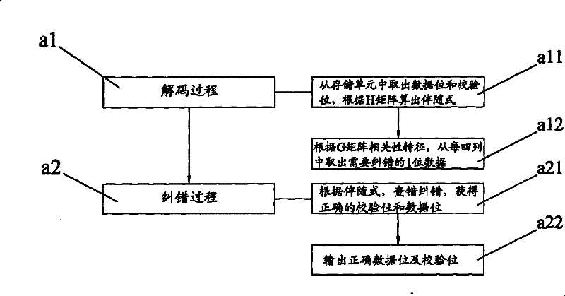
Figure 1 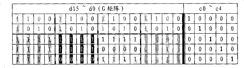
Figure 2 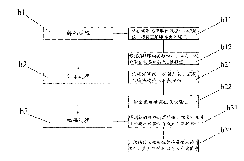
Figure 3
Abstract
Description
technical field
[0001] The present invention relates to a method for implementing ECC in a storage device, in particular to a method for reading data from a memory for error detection and correction, and a method for processing data written into memory by using the above method, and finally to realize the above-mentioned The circuit structures corresponding to the two methods. Background technique
[0002] With the development of integrated circuits, memory cells will occupy most of the chip area. Storage performance has a great impact on chip performance, so it is necessary to ensure 100% accuracy of stored data. However, any memory is faced with the challenges of reliability and yield, such as the decrease of signal-to-noise ratio with the increase of integration density; soft errors caused by cosmic rays to memory cells; process deviation and material defects lead to lower memory yield, etc. Wait. Therefore, an effective method is needed to solve these problems. [00...
Examples
Embodiment Construction
[0047]The above and other technical features and advantages of the present invention will be described in more detail below in conjunction with the accompanying drawings.
[0048] Specific embodiments of the present invention specifically disclose the method and circuit structure, and the corresponding number of stored data for verification is 4 bits;
[0049] see figure 1 As shown, it is a flow chart of the steps of the error checking and error correction method for reading data from the memory in the present invention. The steps it includes are:
[0050] Step a1: a decoding process, wherein the decoding process includes the following steps:
[0051] Step a11: take out the data bit and check bit from the storage unit, and calculate the adjoint formula according to the H matrix;
[0052] Step a12: According to the correlation characteristics of the G matrix, the extracted data bits and check bits are controlled by address information, and the 1-bit data that needs to be corr...