
Silicon carbide mosfet device and manufacturing method thereof
A silicon carbide and device technology, used in semiconductor/solid-state device manufacturing, semiconductor devices, electrical components, etc., can solve problems such as device or ion implanter pollution, device thermal burnout, current amplification, etc., to improve the ability to resist UIS failure, Suppress the effect of opening
Patent Information
- Authority / Receiving Office
- CN · China
- Patent Type
- Patents(China)
- Current Assignee / Owner
- Publication Date
- 2018-11-09
- Estimated Expiration
- Not applicable · inactive patent
Smart Images
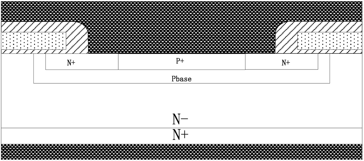
Figure 1 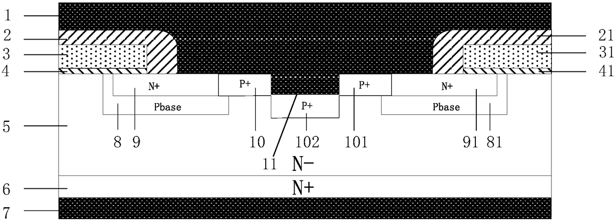
Figure 2 
Figure 3
Abstract
Description
technical field
[0001] The invention belongs to the technical field of power semiconductors, in particular to a silicon carbide MOSFET device and a manufacturing method thereof, which relate to a channel self-alignment process. Background technique
[0002] Silicon carbide (Silicon Carbide) material, as one of the representatives of the third-generation wide bandgap semiconductor materials, has the characteristics of large bandgap width, high critical breakdown electric field, high thermal conductivity and high electron saturation drift velocity, making it suitable for high-power , high temperature and high frequency power electronics has broad application prospects.
[0003] Silicon carbide MOSFET has low on-resistance and small switching loss, which is more suitable for high-frequency operation. In addition, it also has excellent electrical characteristics in high-temperature regions, and has gradually become a new generation of mainstream low-loss power devices.
[0004] ...
Examples
Embodiment Construction
[0043] Embodiments of the present invention are described below through specific examples, and those skilled in the art can easily understand other advantages and effects of the present invention from the content disclosed in this specification. The present invention can also be implemented or applied through other different specific implementation modes, and various modifications or changes can be made to the details in this specification based on different viewpoints and applications without departing from the spirit of the present invention.
[0044]A silicon carbide MOSFET device, comprising a drain metal 7, an N+ substrate 6 above the drain metal 7, and an N-drift region 5 above the N+ substrate 6; a recess is provided in the middle of the N-drift region 5 Groove 11, the first P-type base region 8 is on the left side of the groove 11, and the second P-type base region 81 is on the right side; a first N+ source region 9 is provided above the first P-type base region 8; The...