
Preparation method of super junction semiconductor device capable of improving avalanche capability
A super-junction semiconductor and device technology, which is applied in the field of super-junction semiconductor device preparation, can solve the problems of increased on-resistance, intensified lateral diffusion, and reduced breakdown voltage, so as to increase the effective width and reduce the doping concentration gradient , reducing the effect of lateral diffusion
Patent Information
- Authority / Receiving Office
- CN · China
- Patent Type
- Patents(China)
- Current Assignee / Owner
- Publication Date
- 2016-08-31
Smart Images
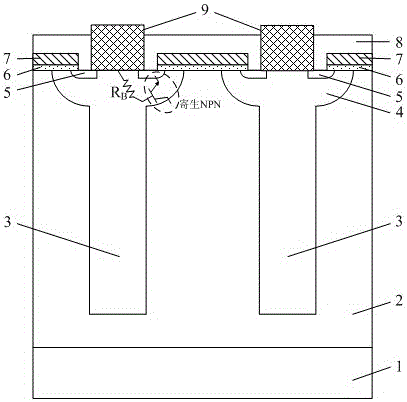
Figure 1 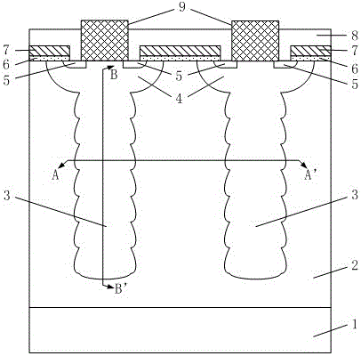
Figure 2 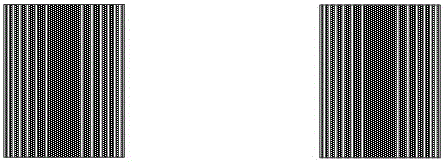
Figure 3
Abstract
Description
technical field
[0001] The invention belongs to the field of semiconductor devices and process manufacturing, and in particular relates to a preparation method of a super junction semiconductor device capable of improving avalanche capability. Background technique
[0002] Super junction VDMOS is a new type of power semiconductor device with rapid development and wide application. It introduces a superjunction (Superjunction) structure on the basis of ordinary vertical double-diffused metal oxide semiconductor (VDMOS), so that it has VDMOS high input impedance, fast switching speed, high operating frequency, voltage control, good thermal stability, and drive The circuit is simple, and overcomes the shortcoming that the on-resistance of VDMOS and the breakdown voltage increase sharply in the relationship of 2.5 powers. At present, super-junction VDMOS has been widely used in power supplies or adapters of consumer electronics products such as computers, mobile phones, lightin...
Examples
Embodiment
[0055] This embodiment is described using a MOSFET having a superjunction structure, but the present invention is not limited to MOSFETs.
[0056] 1. Substrate material preparation, using N with a resistivity of 0.001Ω·cm + Zone-melted single crystal silicon substrate 1, the crystal orientation of which is ;
[0057] Second, in N + A 5 μm N-type epitaxial layer with a resistivity of 4Ω·cm was epitaxially grown on the substrate as the P column and the N-type epitaxial layer. + buffer layer between substrates;
[0058] 3. Epitaxial growth of a 5 μm N-type epitaxial layer with a resistivity of 4Ω·cm on the surface of the silicon wafer;
[0059] 4. Deposit 6 μm negative photoresist on the surface of the silicon wafer (i.e., perform boron ion implantation where there is a P-pillar pattern), use a P-pillar mask to expose and develop, and then perform four high-energy boron ion implantations. The energy of boron ions is 3.5MeV, 2.5MeV, 1.2KeV and 200KeV in sequence, and the dose ...