
A ret IGBT with self-biased pmos and its fabrication method
A self-biasing, split gate technology, applied in semiconductor/solid-state device manufacturing, semiconductor devices, electrical components, etc., can solve problems such as reducing device switching speed, increasing device switching loss, and device breakdown voltage degradation.
Patent Information
- Authority / Receiving Office
- CN · China
- Patent Type
- Patents(China)
- Current Assignee / Owner
- Publication Date
- 2021-04-20
Smart Images
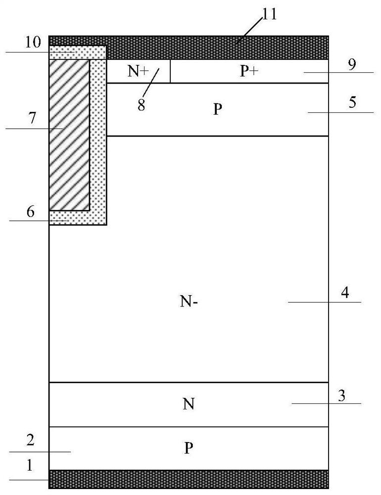
Figure 1 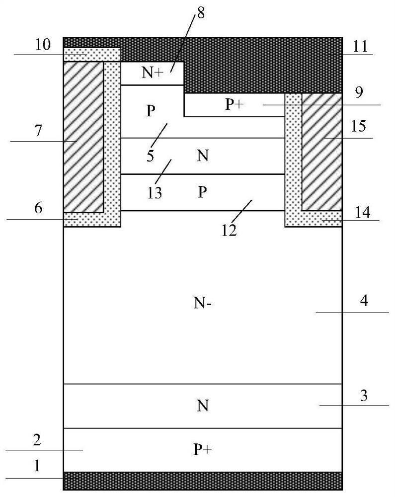
Figure 2 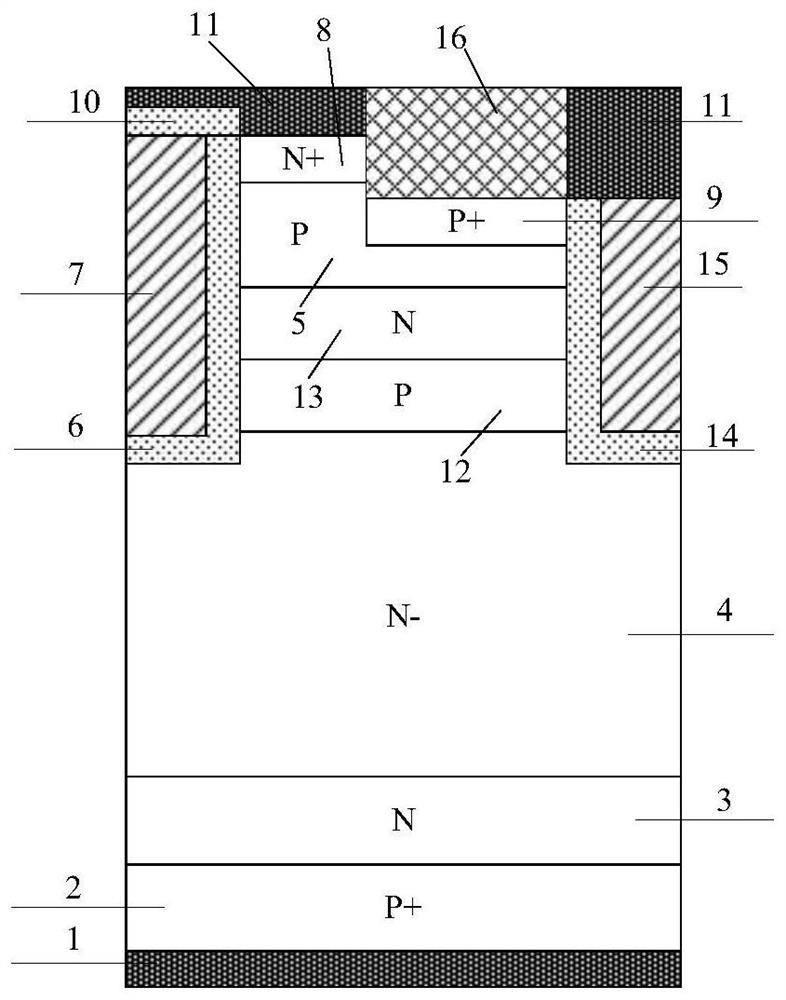
Figure 3
Abstract
Description
technical field
[0001] The invention belongs to the technical field of power semiconductor devices, and relates to an insulated gate bipolar transistor (RET IGBT) with a self-biased PMOS emitter embedded trench. Background technique
[0002] Insulated gate bipolar transistor (IGBT) is a new generation of power electronic devices because it combines the advantages of field effect transistor (MOSFET) and bipolar juncture transistor (BJT). It has the advantages of high speed, and it also has the advantages of large on-state current density, low conduction voltage, low loss and good stability of BJT. Therefore, it has developed into one of the core electronic components in modern power electronic circuits, and is widely used in various fields such as transportation, communication, household appliances and aerospace. The use of IGBT has greatly improved the performance of power electronic systems.
[0003] For more than 30 years since the IGBT came out, how to reduce the switch...
Examples
Embodiment 1
[0051] An embodiment of a RET IGBT device with self-biased PMOS, as figure 2 As shown, it includes: back collector metal 1, P-type collector region 2, N-type field stop layer 3 and N-drift region 4 stacked sequentially from bottom to top, with a trench gate structure above the N-drift region 4 , the trench structure includes a gate dielectric layer 6, a gate electrode 7, and a dielectric layer 10 above the gate dielectric layer 6 and the gate electrode 7; it is characterized in that: a P-type buried layer 12 is placed above the N-drift region 4, A split gate structure, the split gate structure includes a polycrystalline split gate electrode 15, a gate dielectric layer 14; the upper part of the P-type buried layer 12 has an N-type charge storage layer 13; the upper part of the N-type charge storage layer 13 has a P-type base region 5; the upper part of the P-type base region 5 has an N+ emitter region 8 and a P+ contact region 9; 11; the gate electrode 7 is connected to the N-...
Embodiment 2
[0053] An embodiment of a RET IGBT device with self-biased PMOS, as image 3 As shown, it includes: back collector metal 1, P-type collector region 2, N-type field stop layer 3 and N-drift region 4 stacked sequentially from bottom to top, with a trench gate structure above the N-drift region 4 , the trench structure includes a gate dielectric layer 6, a gate electrode 7, a dielectric layer 10 above the gate dielectric layer 6 and the gate electrode 7; it is characterized in that there is a P-type buried layer 12 above the N-drift region 4, separating Gate structure, the separated gate structure includes a polycrystalline separated gate electrode 15, a gate dielectric layer 14; the upper part of the P-type buried layer 12 has an N-type charge storage layer 13; the upper part of the N-type charge storage layer 13 has a P-type base region 5; the upper part of the P-type base region 5 has an N+ emitter region 8 and a P+ contact region 9; The upper part of 9 has a Schottky contact...
Embodiment 3
[0055] An embodiment of a RET IGBT device with self-biased PMOS, as Figure 4 As shown, on the basis of Example 1, a super junction structure composed of super junction N pillars 41 and super junction P pillars 42 is introduced into the drift region, and the junction depth of the super junction P pillars 42 is less than or equal to the junction depth of the super junction N pillars 41. deep, a separate gate electrode 71 is introduced below the gate electrode 71 , and the separate gate electrode 71 is short-circuited with the separate gate electrode 15 .
[0056] The introduction of the super junction structure further reduces the turn-on voltage drop of the device and increases the breakdown voltage of the device, and the introduction of the separated gate electrode 71 further reduces the Miller capacitance of the device.