
Film-forming method for forming passivation film and manufacturing method for solar cell element
Patent Information
- Authority / Receiving Office
- US · United States
- Current Assignee / Owner
- Publication Date
- 2011-12-01
Smart Images
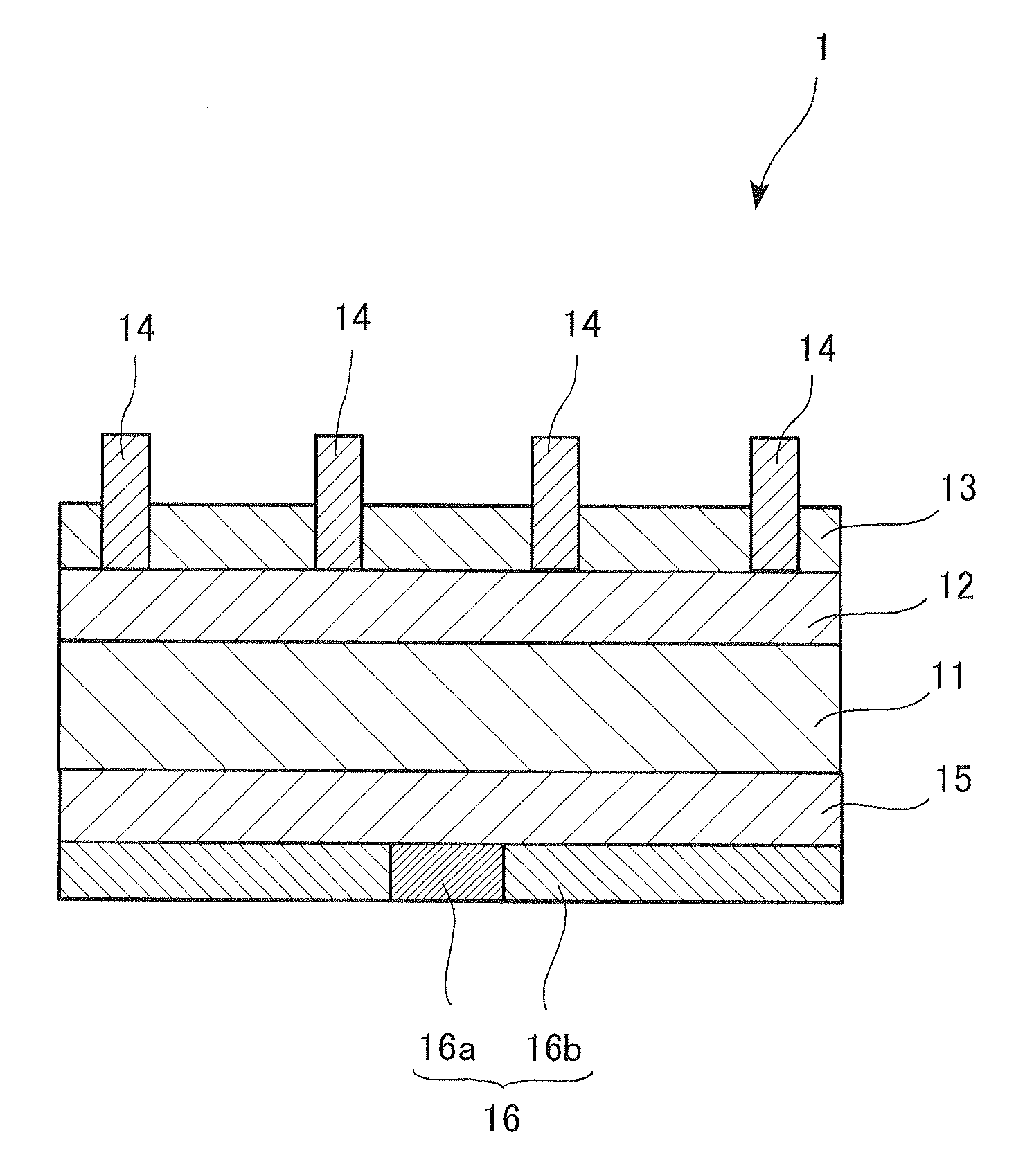
Figure 1 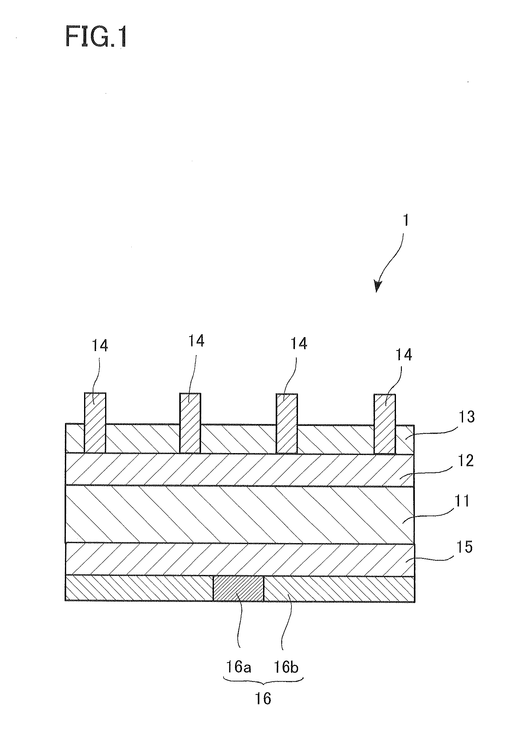
Figure 2 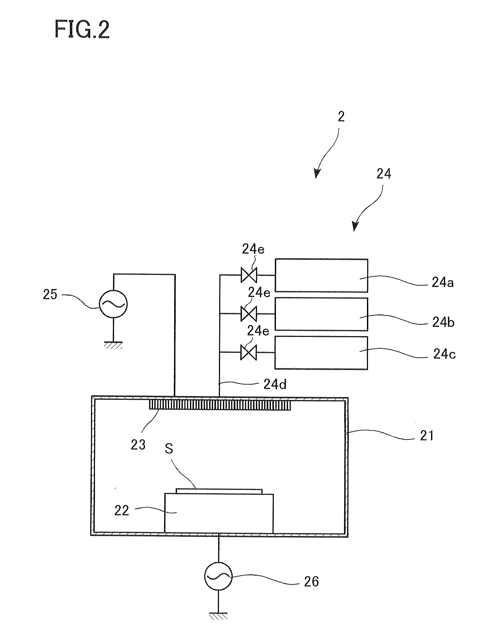
Figure 3
Abstract
Description
CROSS-REFERENCED TO RELATED APPLICATION
[0001] This application is a National Stage entry of International Application No. PCT / JP2009 / 071767, filed on Dec. 28, 2009, which claims priority to Japanese Patent Application 2008-335051, filed Dec. 26, 2008. The disclosure of the prior application is hereby incorporated in its entirety by reference.TECHNICAL FIELD
[0002] This invention relates to a film-forming for a passivation film, and a manufacturing method for a solar cell element.BACKGROUND ART
[0003] A solar cell element, attracting attention as a clean source of energy, is required to reduce a loss in output characteristics for increased output characteristics. The causes of the loss in the output characteristics of the solar cell element include optical losses, for example, a reflection loss and a transmission loss, and electrical losses, for example, the loss of carriers due to their recombination and an ohmic loss.
[0004] Patent Document 1, for example, discloses a solar cell element e...
Examples
example 1
[0039]In the present example, a passivation film was formed using the film-forming device 2 shown in FIG. 2, whereafter a solar cell element was prepared.
[0040]First, an n-type diffusion layer 12 was formed on a surface of a 220 μm thick p-type semiconductor substrate 11 (156 mm×156 mm) of monocrystal silicon having irregularities provided on the surface by texture etching. A plurality of the so treated substrates 11 were arranged side by side on a tray to provide a film-forming object S.
[0041]Then, the film-forming object S was carried into the film-forming device 2 shown in FIG. 2, and a passivation film comprising a silicon nitride film was formed under the following conditions: Substrate temperature: 350° C., SiH4 flow rate: 1500 sccm, NH3 flow rate: 5000 sccm, N2 flow rate: 6000 sccm, frequency of the high frequency power source 25: 13.56 MHz, inputting power of the high frequency power source 25: 1500 W, pressure within the vacuum chamber: 100 Pa, E / S: 14 mm, frequency of the ...
example 2
[0044]In the present example, a solar cell element 1 was produced under exactly the same conditions as those in Example 1, except that the inputting power of the low frequency power source 26 was set at 1000 W.
example 3
[0045]In the present example, a solar cell element 1 was produced under exactly the same conditions as those in Example 1, except that a passivation film was formed using the film-forming device 3 shown in FIG. 3.