
Active device array substrate
a technology of active devices and array substrates, which is applied in the direction of electrical apparatus construction details, vacuum evaporation coating, coatings, etc., can solve the problems of copper oxide formation on the surface of copper, and enlargement accompanied by resistor capacitor delay effects, etc., to achieve better electrical characteristics
Patent Information
- Authority / Receiving Office
- US · United States
- Patent Type
- Patents(United States)
- Current Assignee / Owner
- Publication Date
- 2012-09-18
Smart Images
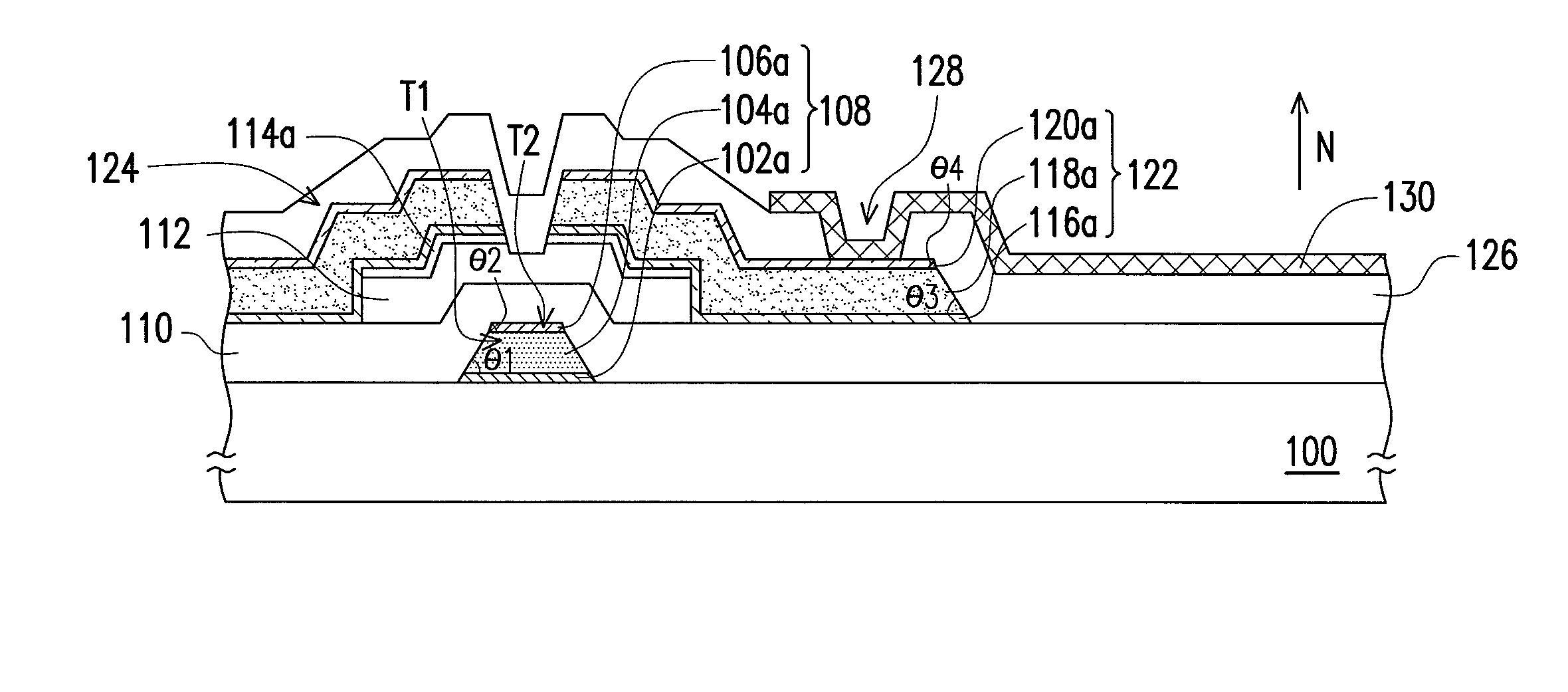
Figure 1 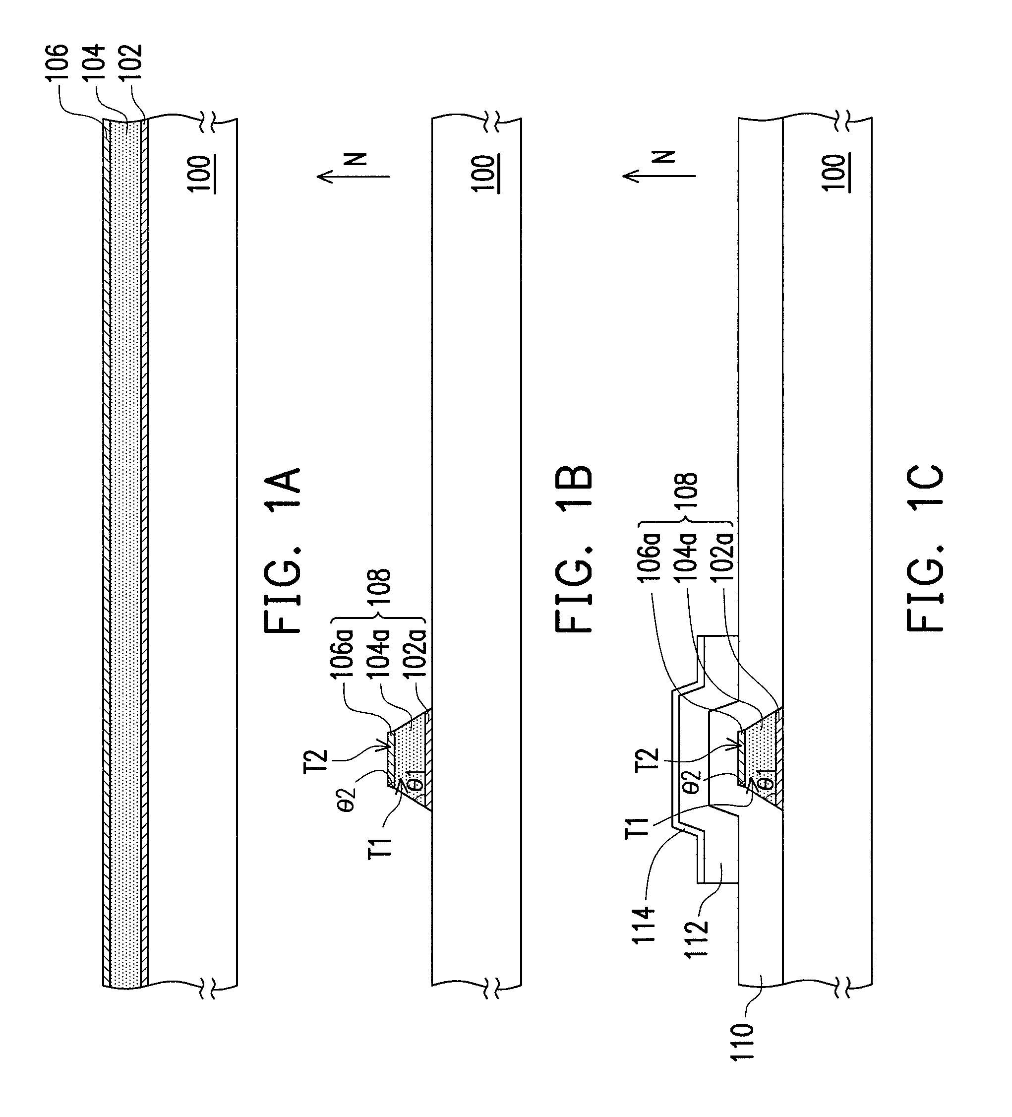
Figure 2 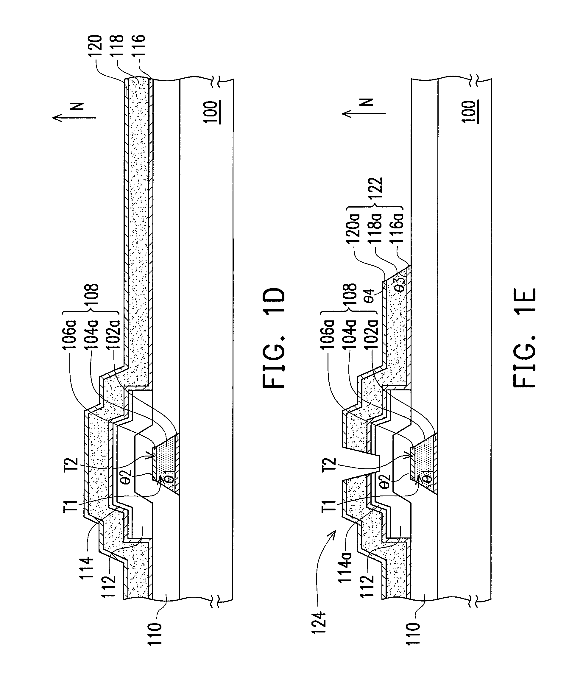
Figure 3
Abstract
Description
CROSS-REFERENCE TO RELATED APPLICATION
[0001] This application claims the priority benefit of Taiwan application serial no. 99108356, filed on Mar. 22, 2010. The entirety of the above-mentioned patent application is hereby incorporated by reference herein and made a part of this specification.BACKGROUND OF THE INVENTION
[0002] 1. Field of the Invention
[0003] The invention is related to an active device array substrate, and in particular to an active device array substrate which has a copper conductive layer.
[0004] 2. Description of Related Art
[0005] As panel sizes of thin film transistor liquid crystal displays (TFT-LCD) become larger and larger, this enlargement is accompanied by resistor capacitor (RC) delay effects caused by resistance values of metal wires which are not low enough. Signals are hence distorted during transmission, thereby affecting the display quality of the panels. By using a single layer of copper which has low resistance as a metal wire, RC delay effects are effectiv...
Examples
Embodiment Construction
[0029]FIGS. 1A to 1G are schematic cross-sectional views showing a fabrication process of an active device array substrate according to an embodiment of the invention. FIG. 2 is a schematic cross-sectional view along another direction of a patterned conductive layer 122 in FIG. 1E, wherein the cross-section direction of FIG. 2 is perpendicular to the cross-section direction of FIG. 1E.
[0030]First, please refer to FIG. 1A. A substrate 100 is provided. The material of the substrate 100 is a transparent material, a non-transparent material, a flexible material, or any combination of the above.
[0031]Next, a barrier layer 102 is optionally / selectively formed on the substrate 100. The material of the barrier layer 102 is at least one selected from the group consisting of molybdenum, a molybdenum alloy, titanium, a titanium alloy, an aluminum alloy, and a copper alloy. The method of forming the barrier layer 102 is, for example, a physical vapor deposition method.
[0032]Next, a copper layer...