Analog signal sampling circuit and switch capacitance circuit
What is AI technical title?
AI technical title is built by Patsnap AI team. It summarizes the technical point description of the patent document.
A sampling circuit and analog signal technology, applied in the electronic field, can solve the problems of signal distortion and inability to achieve high linearity sampling, etc., and achieve the effect of high linearity
Active Publication Date: 2009-11-25
BEIJING VIMICRO ARTIFICIAL INTELLIGENCE CHIP TECH CO LTD
View PDF2 Cites 15 Cited by
Summary
Abstract
Description
Claims
Application Information
AI Technical Summary
This helps you quickly interpret patents by identifying the three key elements:
Problems solved by technology
Method used
Benefits of technology
Problems solved by technology
However, in the above-mentioned sampling circuit, since the conduction voltage of the sampling switch (that is, the voltage between the gate and the source) is related to the input signal and changes with the input signal, the conduction resistance of the sampling switch also changes with the signal. Causes the sampled signal to be distorted, and high linearity sampling cannot be achieved
Method used
Image
Click on the blue label to locate the original text in one second.
Reading with bidirectional positioning of images and text.
Examples
Embodiment 1
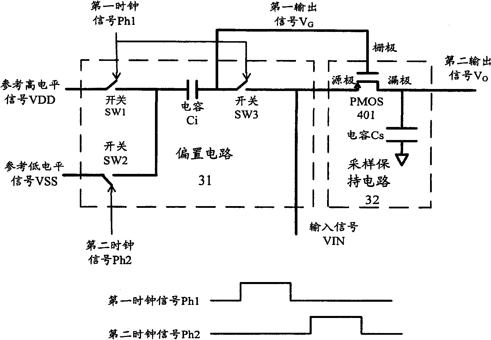
[0042] refer to Figure 4 , shows a structural diagram of an analog signal sampling circuit described in the embodiment.
[0043] The analog signal sampling circuit described in this embodiment includes switches SW4, SW5, capacitors Cs, Cint and operational amplifier A1, wherein:
[0044] The switch SW4 is controlled by the clock PH1, one end is connected to the node n1, and the other end is connected to the reference voltage;
[0045] The switch SW5 is controlled by the clock PH2, one end is connected to the node n1, and the other end is connected to the inverting input end of the operational amplifier A1;
[0046] The non-inverting input terminal of the operational amplifier A1 is connected to the reference voltage, and the integrating capacitor Cint is connected in parallel between the inverting input terminal and the output terminal;
[0047] Capacitor Cs is connected between node n1 and node n2 as a sampling capacitor;
[0048] The analog signal sampling circuit also i...
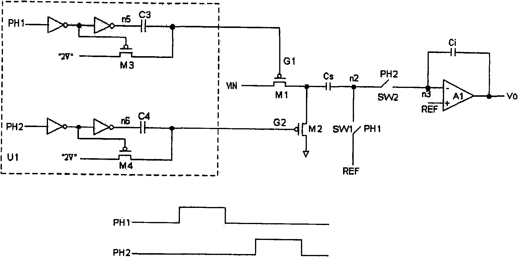
Embodiment 2
[0074] This embodiment will describe a switched capacitor circuit of the present invention in detail.
[0075] Switched capacitor circuits usually use MOS technology, the process is relatively simple, and it is easy to integrate on a large scale, so it has developed rapidly in the field of electronic technology and is widely used in various integrated circuits, such as filter circuits, integrating circuits and sampling circuit etc. At present, the accuracy of signal processing in integrated circuits is getting higher and higher. Therefore, the requirements for switched capacitor circuits in practical applications are also getting higher and higher, especially for the linearity of circuits. Sometimes, it is also required to process input signals lower than the lowest voltage in the circuit.
[0076] The switched capacitor circuit of the present invention, by setting a voltage constant module, can make the voltage value between the gate and the source of the switch constant whe...
PUM
Abstract
The present invention provides an analog signal sampling circuit capable of enabling the circuit to have high linearity, meanwhile, the processing of signal less than the minimum voltage in the circuit can be implemented. The analog signal sampling circuit can generate the constant voltage by arranging the voltage constant module as a voltage between gate source poles when the PMOSFET tube of the switch tube is conductive, the voltage between the grid and the source pole can be kept constant without changing with the variation of the input signal when the PMSFET tube is in the conducting state, the conductive electric resistance of the PMOSFET tube can not change following with the variation of the input signal, at last the PMOSFET has constant conductive electric resistance, the signal distortion through the PMOSFET tube is smaller, the high linearity sampling can be implemented. The invention also provides a switch capacitance circuit.
Description
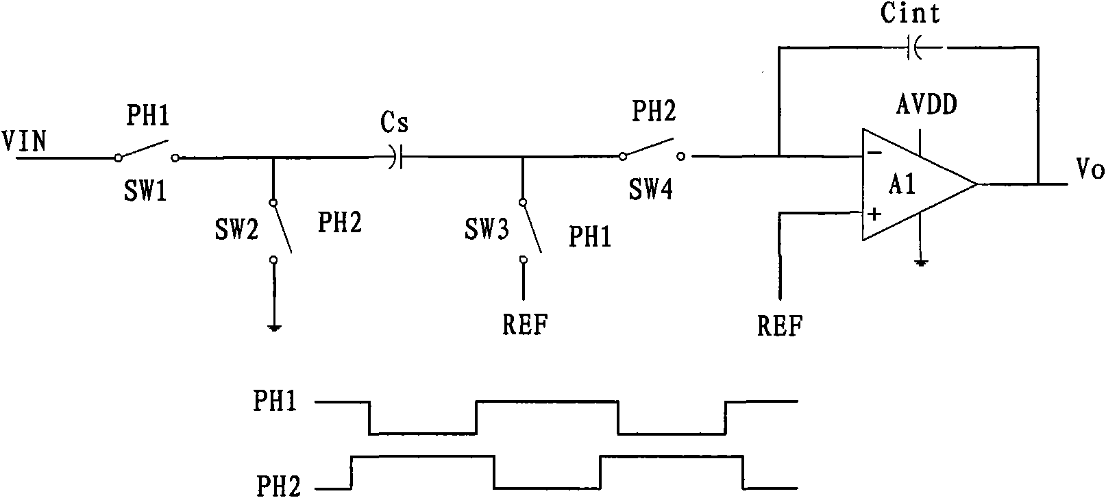
technical field [0001] The invention relates to the field of electronic technology, in particular to an analog signal sampling circuit and a switched capacitor circuit. Background technique [0002] Switched Capacitor Circuit (Switched Capacitor Circuit) is a circuit basically composed of a switch and a capacitor controlled by a clock signal; it uses the storage and transfer of charges to realize various processing functions for signals. In actual circuits, sometimes the circuits based on switches and capacitors cannot meet the requirements, so switched capacitor circuits are often combined with amplifiers or operational amplifiers, comparators, etc. to realize the generation, transformation and processing of electrical signals. [0003] In common analog signal sampling circuits, sample and hold circuits usually use MOS switched capacitor circuits to implement various signal processing functions, for example, figure 1 The sampling circuit shown. In the usual CMOS process, ...
Claims
Application Information
Patent Timeline
Application Date:The date an application was filed.
Publication Date:The date a patent or application was officially published.
First Publication Date:The earliest publication date of a patent with the same application number.
Issue Date:Publication date of the patent grant document.
PCT Entry Date:The Entry date of PCT National Phase.
Estimated Expiry Date:The statutory expiry date of a patent right according to the Patent Law, and it is the longest term of protection that the patent right can achieve without the termination of the patent right due to other reasons(Term extension factor has been taken into account ).
Invalid Date:Actual expiry date is based on effective date or publication date of legal transaction data of invalid patent.
IPC IPC(8): G11C27/02H03K17/687
CPCH03M1/00G11C27/026
Inventor龚川
OwnerBEIJING VIMICRO ARTIFICIAL INTELLIGENCE CHIP TECH CO LTD

