Liquid crystal panel and manufacturing method thereof

A liquid crystal panel and display substrate technology, applied in nonlinear optics, instruments, optics, etc., to achieve the effect of increasing vertical distance and reducing parasitic capacitance

Active Publication Date: 2011-03-30
BOE TECH GRP CO LTD +1
View PDF0 Cites 30 Cited by
  • Summary
  • Abstract
  • Description
  • Claims
  • Application Information

AI Technical Summary

Problems solved by technology

However, the problem with this solution is that the thickness of the passivation layer needs to be more than 2 microns (μm), so that the parasitic capacitance can be reduced to meet the requirements when the distance between the pixel e

Method used


Image

  • Liquid crystal panel and manufacturing method thereof
  • Liquid crystal panel and manufacturing method thereof
  • Liquid crystal panel and manufacturing method thereof

Examples


Embodiment 1

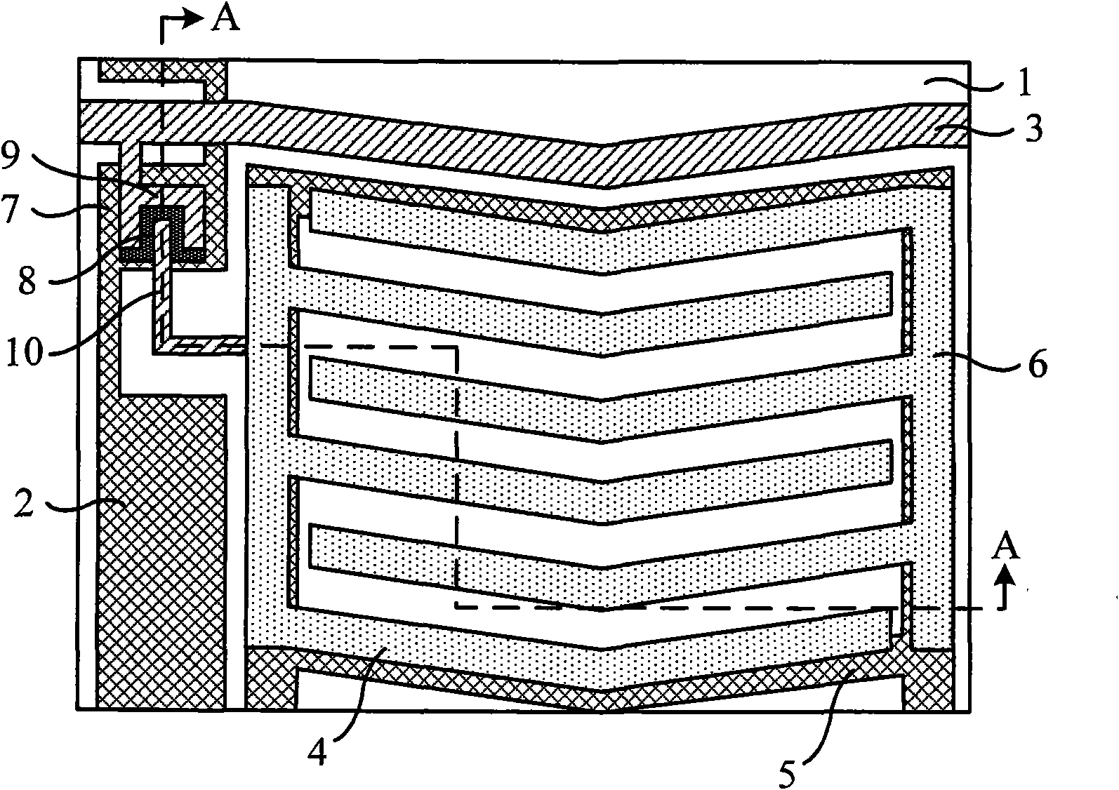
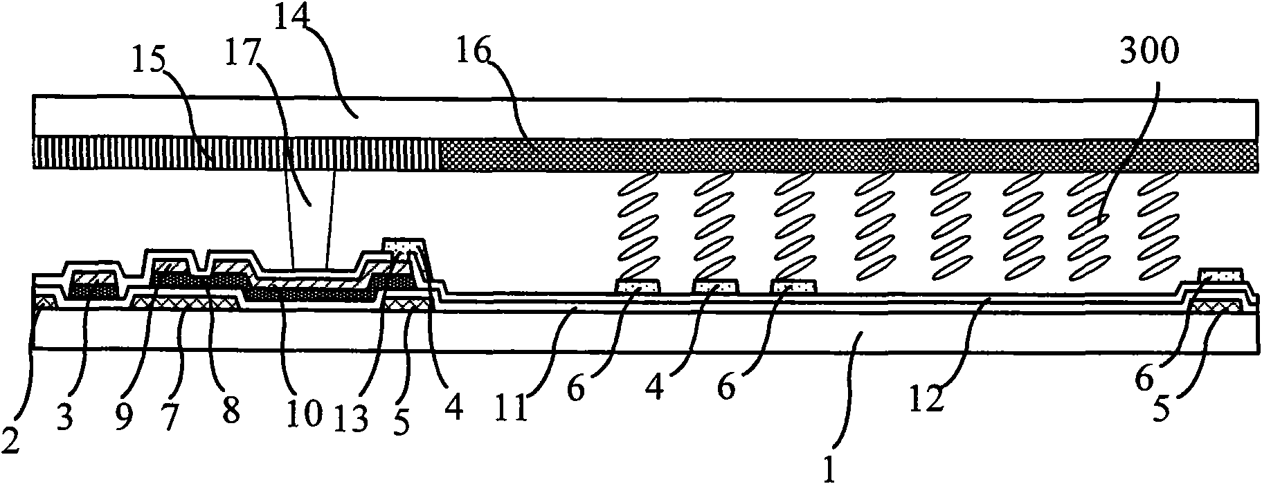
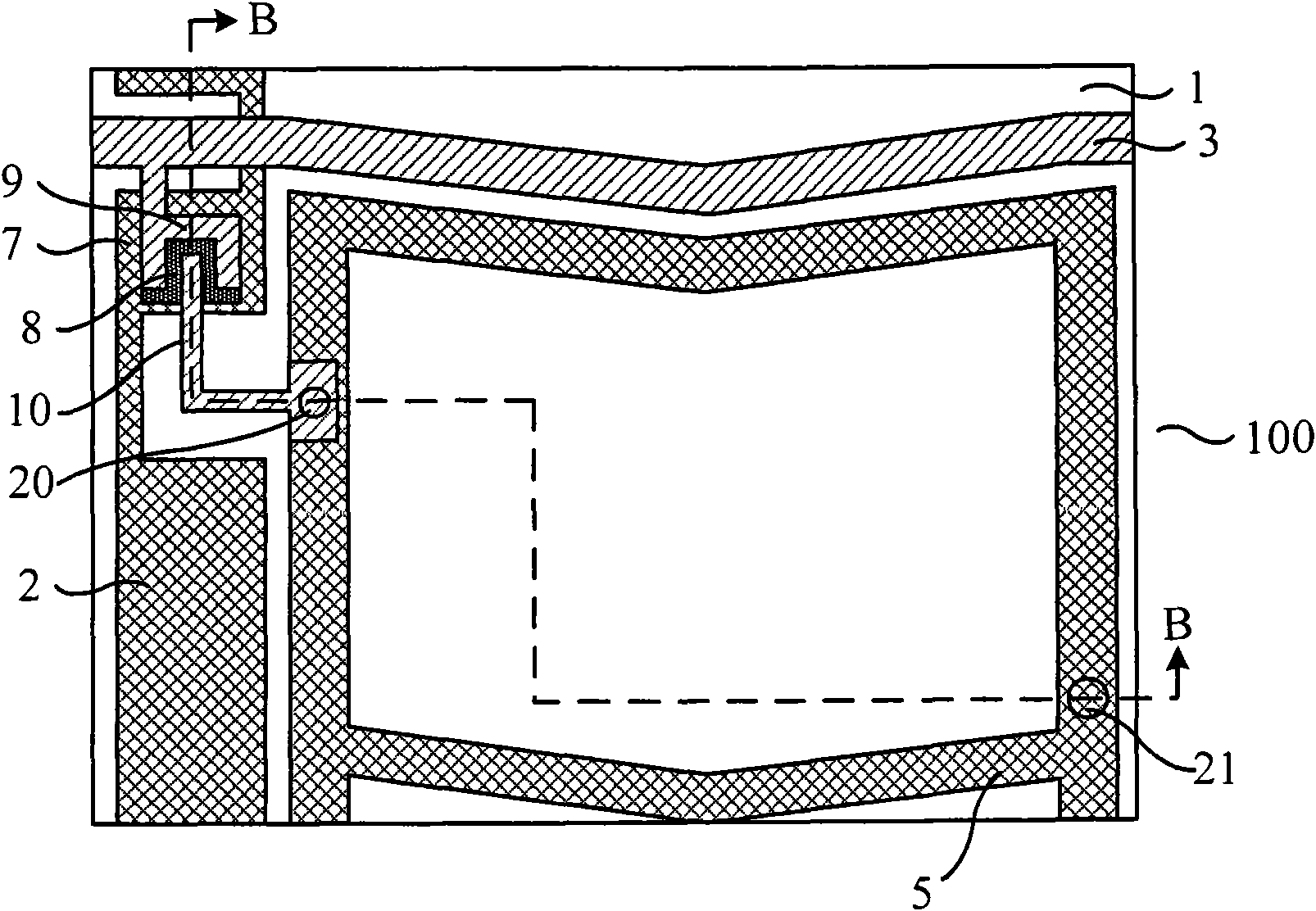
[0066] image 3 It is a partial top view structural schematic diagram of the first display substrate in the liquid crystal panel provided by Embodiment 1 of the present invention, Figure 4 It is a partial top view structural schematic diagram of the second display substrate in the liquid crystal panel provided by Embodiment 1 of the present invention, Figure 5 It is a schematic diagram of a partial side-view cross-sectional structure of a liquid crystal panel provided in Embodiment 1 of the present invention, Figure 5 for along image 3 The B-B line in and Figure 4 Obtained by sectioning the C-C line in . The liquid crystal panel of this embodiment includes a first display substrate 100 and a second display substrate 200 arranged opposite to each other, and a liquid crystal 300 is filled between the first display substrate 100 and the second display substrate 200 .

[0067] The first display substrate 100 specifically includes a first base substrate 1 , on which a plur...

Embodiment 2

[0074] Figure 6 It is a partial top view structural schematic diagram of the first display substrate in the liquid crystal panel provided by Embodiment 2 of the present invention, Figure 7 It is a partial top view structural schematic diagram of the second display substrate in the liquid crystal panel provided by Embodiment 2 of the present invention, Figure 8 It is a schematic diagram of a partial side-view cross-sectional structure of a liquid crystal panel provided in Embodiment 2 of the present invention, Figure 8 for along Figure 6 The D-D line in and Figure 7 Obtained by sectioning the E-E line in . The difference between this embodiment and Embodiment 1 is that the common electrode lines 5 are formed on the second base substrate 14, and the common electrode lines 5 are covered with a common electrode insulating layer 23, and the pixel electrodes 4 and the common electrodes 6 are formed on the common electrode lines. On the insulating layer 23 , a third via hol...

Embodiment 3

[0077] Figure 9 It is a partial top view structural schematic diagram of the second display substrate in the liquid crystal panel provided by Embodiment 3 of the present invention, Figure 10 It is a schematic diagram of a partial side-view cross-sectional structure of a liquid crystal panel provided in Embodiment 3 of the present invention, Figure 10 for along Figure 9 The F-F line in the section is obtained, and Figure 10 3 shows the first display substrate 100 and the liquid crystal 300 . The difference between this embodiment and the above-mentioned second embodiment is that the second embodiment is an IPS mode LCD in which the pixel electrode 4 and the common electrode 6 are formed on the same layer. interval, and the pixel electrode 4 has a comb pattern with multiple slits, and the common electrode 6 is an FFS mode LCD with a block pattern corresponding to the pixel unit area.

[0078] In this embodiment, the structure of the first display substrate 100 can refer...


PUM


Abstract

The invention relates to a liquid crystal panel and a manufacturing method thereof. The liquid crystal panel comprises two display substrates capable of being perfectly bonded together, wherein raster scanning lines and data lines are formed on the first display substrate, and enclose to form a pixel unit; a thin film transistor (TFT) is arranged in the pixel unit; a pixel electrode and a common electrode are respectively formed in each pixel area of the second lining substrate; a first pad object containing a conducting material is formed between the first display substrate and the second display substrate, and connects the pixel electrode on the second display substrate and a drain electrode exposed through a first hole; and a common electrode line is formed on the first lining substrate or the second lining substrate, and is electrically connected with the common electrodes. A technical means of separately arranging the pixel electrodes and the common electrodes forming a horizontal field and the data lines on the two display substrates is adopted, and the parasitic capacitance between the pixel electrodes and the data lines cannot be improved when adjacent pixel electrodes are close to each other.

Description

technical field [0001] Embodiments of the present invention relate to liquid crystal display technology, and in particular to a liquid crystal panel and a manufacturing method thereof. Background technique [0002] In order to improve the wide viewing angle characteristics of liquid crystal displays (Liquid Crystal Display; hereinafter referred to as: LCD), especially the contrast ratio (Contrast Ratio; hereinafter referred to as: CR) of various viewing angles in the field of TV display, that is, the high requirements for wide viewing angle characteristics, currently proposed LCD in horizontal electric field mode. The LCD in the horizontal electric field mode mainly includes an In-Plane Switching (hereinafter referred to as: IPS) mode and a fringe field switching (Fringe Field Switching; hereinafter referred to as: FFS) mode and the like. The feature of the horizontal electric field technology is that a horizontal electric field is formed between the pixel electrode and the...

Claims


Application Information

Patent Timeline
IPC IPC(8): G02F1/1333G02F1/1343G02F1/1345G02F1/1362G02F1/1368
Inventor 闵泰烨王章涛邱海军
Owner BOE TECH GRP CO LTD
Why Eureka
Try Eureka