Check patentability & draft patents in minutes with Patsnap Eureka AI!

Transparent multi-layer circuit board

A multi-layer circuit and circuit board technology, applied in the direction of printed circuit components, etc., can solve problems such as scrap, defective, and lack of transparency, and achieve the effect of reducing abnormal hole deviation, reducing material waste, and feeding materials in advance.

Inactive Publication Date: 2012-12-12
TIGERBUILDER CIRCUIT SUZHOU
View PDF0 Cites 2 Cited by
  • Summary
  • Abstract
  • Description
  • Claims
  • Application Information

AI Technical Summary

Problems solved by technology

[0002] During the production process of multilayer circuit boards, multiple circuits and laminations are required. Therefore, the inner circuit part will be laminated to the inside of the multilayer circuit board again. At present, the insulating material used in circuit boards is mainly epoxy The resin is mixed with some inorganic fillers, and its material properties do not have transparency. In the subsequent production process, the interior of the multilayer circuit board cannot be observed. For example, abnormal drilling deviation of the drilled holes, and abnormal opening and short circuit of the inner layer circuit cannot be observed. However, technicians cannot make a judgment, and often flow abnormal boards into the next process, and finally form defective products and cause excessive scrapping

Method used


Image

  • Transparent multi-layer circuit board

Examples


Embodiment Construction

[0011] The present invention is described below in conjunction with accompanying drawing.

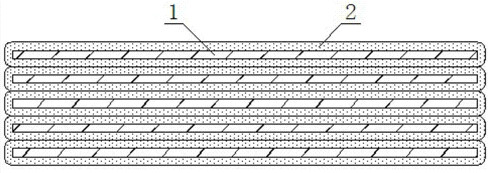
[0012] attached figure 1 It is a kind of transparent multilayer circuit board according to the present invention, which includes a multilayer circuit board body and an insulating layer 2; the multilayer circuit board body is formed by stacking a plurality of single-layer circuit boards 1; the insulating layer 2 Uniformly arranged on every single-layer circuit board 1; the thickness of the insulating layer 2 is 1 mm to 2 mm; the material of the insulating layer 2 is polymer transparent insulating ink.

[0013] Due to the application of the above-mentioned technical solution, the present invention has the following advantages compared with the prior art:

[0014] The transparent multilayer circuit board of the present invention uses polymer transparent insulating ink to replace the traditional epoxy resin prepreg, so technicians can observe the inside of the multilayer circuit board, and...


PUM


Abstract

The invention discloses a transparent multi-layer circuit board which comprises a multi-layer circuit board body and an insulating layer, wherein the multi-layer circuit board body is formed by overlaying a plurality of single-layer circuit boards; the insulating layer is uniformly arranged at each position on each single-layer circuit board; and the insulating layer is made of high-polymer transparent insulating ink. According to the transparent multi-layer circuit board, the high-polymer transparent insulating ink is adopted to replace the traditional epoxy resin prepreg, and technical personnel can observe the inside of the multi-layer circuit board and evaluate the drilling hole deviation. In the drilling manufacture procedure, hole deviation abnormality is reduced, parts of line problems can be detected from high-polymer insulating material, scraps are carried out in advance, the material waste of the subsequent manufacture procedure is reduced, and feed supplement processing is carried out in advance.

Description

technical field [0001] The invention relates to a multilayer circuit board, in particular to a transparent multilayer circuit board which is convenient for personnel to observe the inner layer, and belongs to the technical field of electronic components. Background technique [0002] During the production process of multilayer circuit boards, multiple circuits and laminations are required. Therefore, the inner circuit part will be laminated to the inside of the multilayer circuit board again. At present, the insulating material used in circuit boards is mainly epoxy The resin is mixed with some inorganic fillers, and its material properties do not have transparency. In the subsequent production process, the interior of the multilayer circuit board cannot be observed. For example, abnormal drilling deviation of the drilled holes, and abnormal opening and short circuit of the inner layer cannot be observed. It is found that technicians cannot make a judgment, and often flow ab...

Claims


Application Information

Patent Timeline
Patent Type & Authority Applications(China)
IPC IPC(8): H05K1/02
Inventor 卢耀普
Owner TIGERBUILDER CIRCUIT SUZHOU
Features
  • R&D
  • Intellectual Property
  • Life Sciences
  • Materials
  • Tech Scout
  • Unparalleled Data Quality
  • Higher Quality Content
  • 60% Fewer Hallucinations
Learn More