communication device

A communication device and conduction technology, which is applied in the direction of antenna grounding device, radiation element structure, etc., can solve the problems of internal space size limitation and other problems

CN103872433BActive Publication Date: 2016-09-07ACER INC
2 Cites 0 Cited by

Patent Information

Authority / Receiving Office
CN · China
Patent Type
Patents(China)
Current Assignee / Owner
Publication Date
2016-09-07

Smart Images

  • Figure 1
    Figure 1
  • Figure 2
    Figure 2
  • Figure 3
    Figure 3
Patent Text Reader

Abstract

The invention provides a communication device, comprising a grounding element, an antenna element and a switching unit. In nature, the antenna element is a loop antenna and comprises a first portion, a second portion and a third portion. The first portion is electrically connected to a signal source; the second portion comprises (N-1) bends to form N connection sections; and the third portion comprises (P-1) bends to form P grounding sections, wherein N and P are integer larger than 1. The N connection sections are connected between a first terminal of the first grounding section and the first portion in series. A second terminal of the ith grounding section is electrically connected to a first terminal of the (i+1)th grounding section, wherein i is an integer equal to or larger than 1 and small than or equal to (P-1). A second terminal of the Pth grounding section is electrically connected to the grounding element; the (P-1)th grounding section comprises at least one grounding point. The switching unit is electrically connected between at least one grounding point and the grounding element.
Need to check novelty before this filing date? Find Prior Art

Description

technical field

[0001] The present invention relates to a communication device, especially a mobile communication device with a reconfigurable antenna element. Background technique

[0002] In recent years, due to the rapid progress of wireless communication technology, people no longer only use communication as the main purpose of communication devices, but have more functional and diversified demands. In order to meet people's needs, mobile phones must be equipped with more components and modules. Under the premise that the current communication device must be light and thin, its internal space is limited to a certain size. Therefore, the limited design space in a communication device is at a premium. In view of this, in the antenna design of communication devices, how to make the most effective use of the limited antenna design space is a very important issue. Contents of the invention

[0003] The present invention provides a communication device that uses a switchi...

Examples

Embodiment Construction

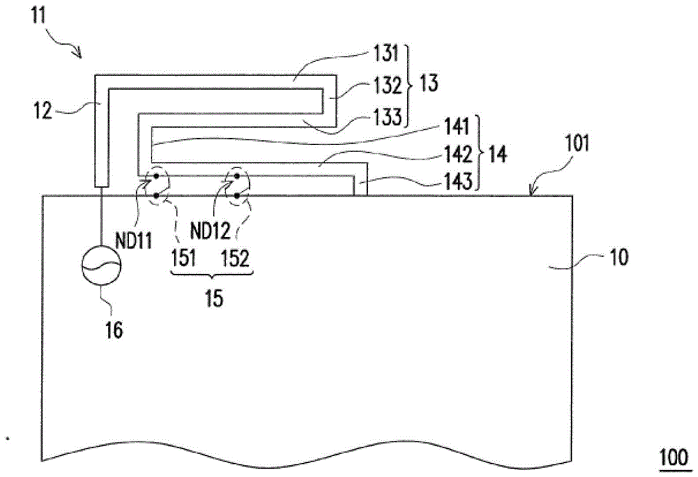
[0031] figure 1 It is a schematic structural diagram of the communication device shown in the first embodiment of the present invention. The communication device 100 includes a ground element 10 , an antenna element 11 and a switching unit 15 . The antenna element 11 is essentially a loop antenna and is adjacent to the ground element 10 . Furthermore, the antenna element 11 includes a first part 12 , a second part 13 and a third part 14 . Wherein, the first part 12 is electrically connected to a signal source 16 .

[0032] In this embodiment, the second part 13 has two bends, and three connecting sections 131 - 133 are formed by the two bends. Similarly, the third part also has two bends, and three grounding sections 141 - 143 are formed by the two bends. Wherein, the connecting sections 131 - 133 are connected in series between the first end of the first grounding section 141 and the grounding element 10 . Wherein, the sum of the lengths of the first connecting section 1...