
Data storage method and device
A data storage and data technology, which is applied in memory system, electrical digital data processing, memory address/allocation/relocation, etc., can solve the problems of space occupation, increase of production cost of NandFlash storage device, etc., so as to save production cost and cache effect of space
- Summary
- Abstract
- Description
- Claims
- Application Information
AI Technical Summary
Problems solved by technology
Method used
Image

Examples
no. 1 example
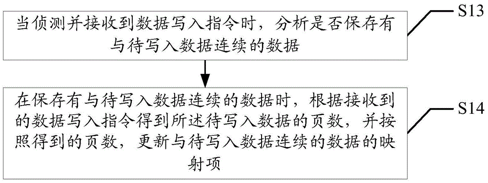
[0070] Based on the above-mentioned first embodiment, the method also includes the steps of:
[0071] Step S13, when the data writing instruction is detected and received, analyze whether there is data continuous with the data to be written;
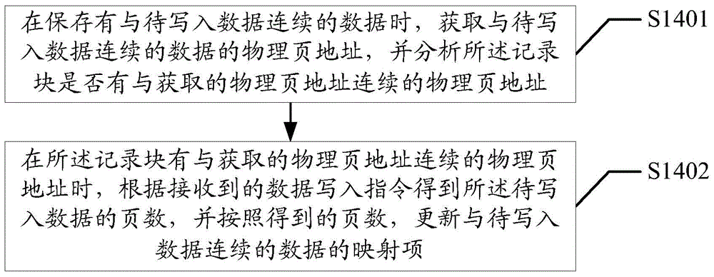
[0072] Step S14, when the data continuous with the data to be written is stored, obtain the page number of the data to be written according to the received data write command, and update the page number continuous with the data to be written according to the obtained page number A map entry for the data.
[0073] Refer to Table 6, the logical page address corresponding to the data to be written is 0x00000005, single logical page data is one page of data, refer to Table 2, it is the mapping table of the saved data, and exists in the mapping table of the saved data The logical page address is 0x00000004, which is analyzed to obtain data that is continuous with the data to be written. According to the received data write command, the numbe...
no. 2 example
[0083] Based on the first and second embodiments above, the method also includes the steps of:
[0084] Step S15, when the data write command is detected and received, determine the logical page address of the data to be written according to the received data write command, and determine the corresponding logical page address for each logical page address of the data to be written physical page address, and analyze whether there is data consistent with the logical page address of the data to be written;
[0085] Step S16, when the data consistent with the logical page address of the data to be written is stored, find out the mapping item corresponding to the data consistent with the logical page address of the data to be written, and update and find out according to the determined physical page address mapping item.
[0086] Referring to Table 6, the logical page address corresponding to the data to be written is 0x00000005, and the determined physical page address is 0x00001...
PUM
 Abstract
Description
Claims
Application Information