Parallel fiber array and photoelectron chip coupling component

An optoelectronic chip and fiber array technology, which is applied to the coupling of optical waveguides and other directions, can solve the problems of inconvenient adjustment and observation of lens arrays, difficult optical fiber coupling alignment and observation, and unfavorable integration, etc., and achieves easy coupling, alignment, and fixation. Easy, reliable results

Inactive Publication Date: 2015-04-29
武汉耀晟互连科技有限公司
View PDF7 Cites 12 Cited by
  • Summary
  • Abstract
  • Description
  • Claims
  • Application Information

AI Technical Summary

Problems solved by technology

However, by processing the end face of each fiber of the fiber array to make the end face 45° optical plane relative to the fiber axis, the processing cost is high, and the observation of fiber coupling alignment is not easy
The method of aligning through the lens array is inconvenient to adjust and observe the alignment of the lens array, and the equipment is more complicated, which is not conducive to further integration.

Method used


Image

  • Parallel fiber array and photoelectron chip coupling component
  • Parallel fiber array and photoelectron chip coupling component
  • Parallel fiber array and photoelectron chip coupling component

Examples


Embodiment Construction

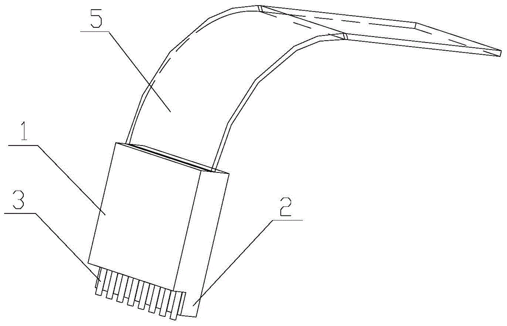
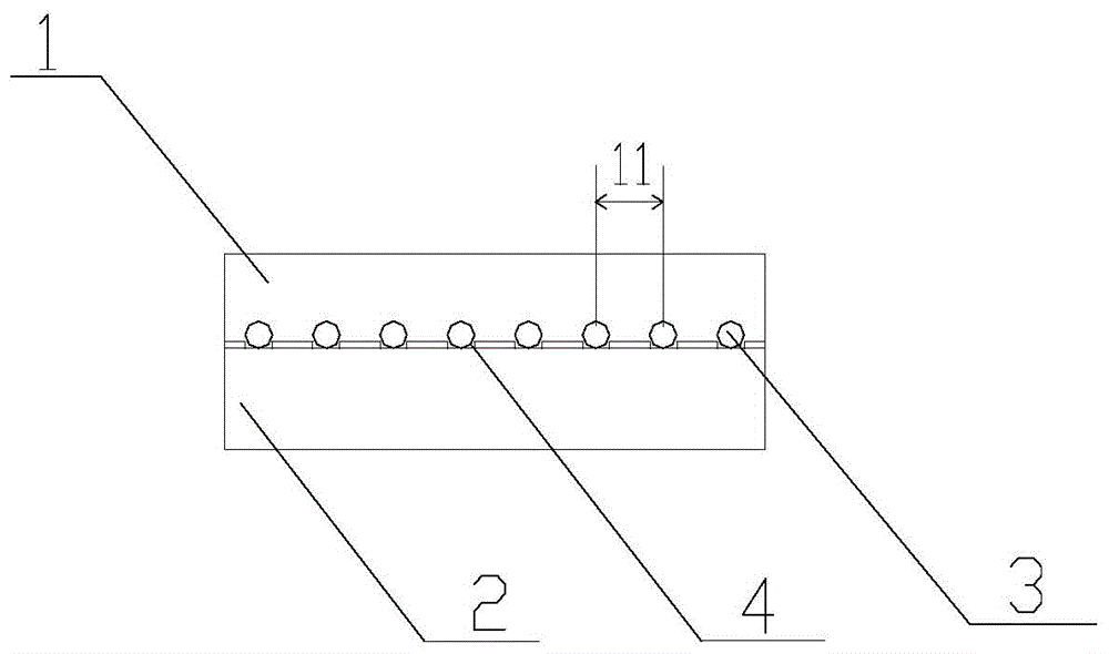
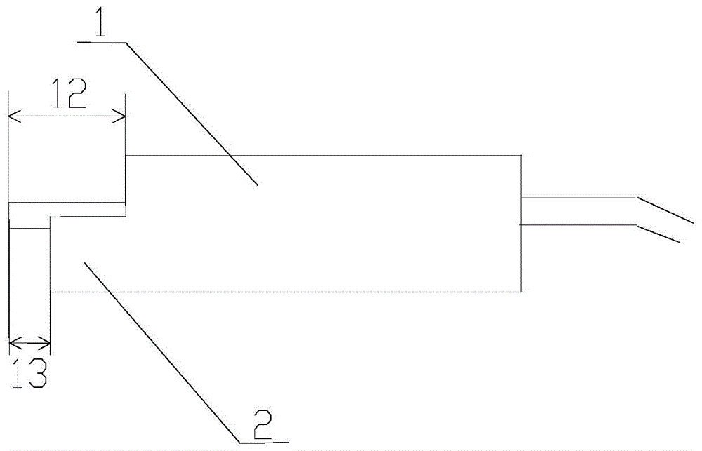
[0027] The invention is a structure in which the parallel optical fiber array is directly coupled with the surface emitting laser array VCSEL chip or the array detector PIN chip. The coupling assembly of the parallel optical fiber array of the present invention comprises base, optical fiber array and PCB circuit board, and its key point has: (1) described circuit board also comprises parallel emitting laser array VCSEL chip or array detector PIN or GaAs chip, ( 2) The exposed fiber core at the end of the parallel fiber array is directly cut by a parallel fiber cutter, and each fiber core of the fiber array is connected to each pixel of the parallel emission laser array VCSEL chip or each pixel of the array detector PIN or GaAs chip One-to-one alignment.

[0028] Described parallel light array coupling assembly, its main point also has: (3) parallel optical fiber array directly cut by parallel optical fiber cutter and corresponding parallel emission laser array VCSEL chip pixel...


PUM


Abstract

The invention provides a parallel fiber array and a photoelectron chip coupling component. The coupling component includes a printed circuit board (6), a photoelectron chip (8), a fiber array module (5) and a base (7), wherein the photoelectron chip (8) is arranged on the printed circuit board (6), head ends of the fiber array module (5) is aligned with each pixel of the photoelectron chip (8), the fiber array module (5) is arranged on the base (7), and the base (7) is fixed with the printed circuit board (6). The parallel fiber array and a photoelectron chip coupling component has the advantages of simple structure, good coupling performance and high reliability.

Description

technical field [0001] The invention belongs to optoelectronic devices in the field of optical communication, parallel processing computer, etc., and in particular relates to an optical fiber array component with interface for coupling input and output parallel channels of active and passive optoelectronic chips in the field of optical communication, parallel processing computer, etc. Background technique [0002] In recent years, due to the rapid development of clusters and network computing systems in the optical communication and computer fields, the communication capacity has increased sharply. Under this situation, large capacity is no longer the only goal pursued, and the issue of communication speed has attracted more and more attention. Especially in some high-speed systems, the demand for parallel optical communication is also increasing. Driven by a strong market, a large number of new active devices and passive devices used in the information field have emerged. ...

Claims


Application Information

Patent Timeline
Patent Type & Authority Applications(China)
IPC IPC(8): G02B6/43
CPCG02B6/43
Inventor 徐军熊志强钱银博李晓磊刘德明
Owner 武汉耀晟互连科技有限公司
Why Eureka
Try Eureka