Array substrate and manufacturing method thereof, and display device

A technology for array substrates and manufacturing methods, which is applied in the display field and can solve problems such as low light transmittance of array substrates

Active Publication Date: 2016-08-03
BOE TECH GRP CO LTD
View PDF4 Cites 4 Cited by
  • Summary
  • Abstract
  • Description
  • Claims
  • Application Information

AI Technical Summary

Problems solved by technology

[0004] The object of the present invention is to provide an array substrate and its manufacturing method, and a display device to solve the problem of low light transmittance of the array substrate adopting a comb electrode structure

Method used


Image

  • Array substrate and manufacturing method thereof, and display device
  • Array substrate and manufacturing method thereof, and display device
  • Array substrate and manufacturing method thereof, and display device

Examples


Embodiment 1

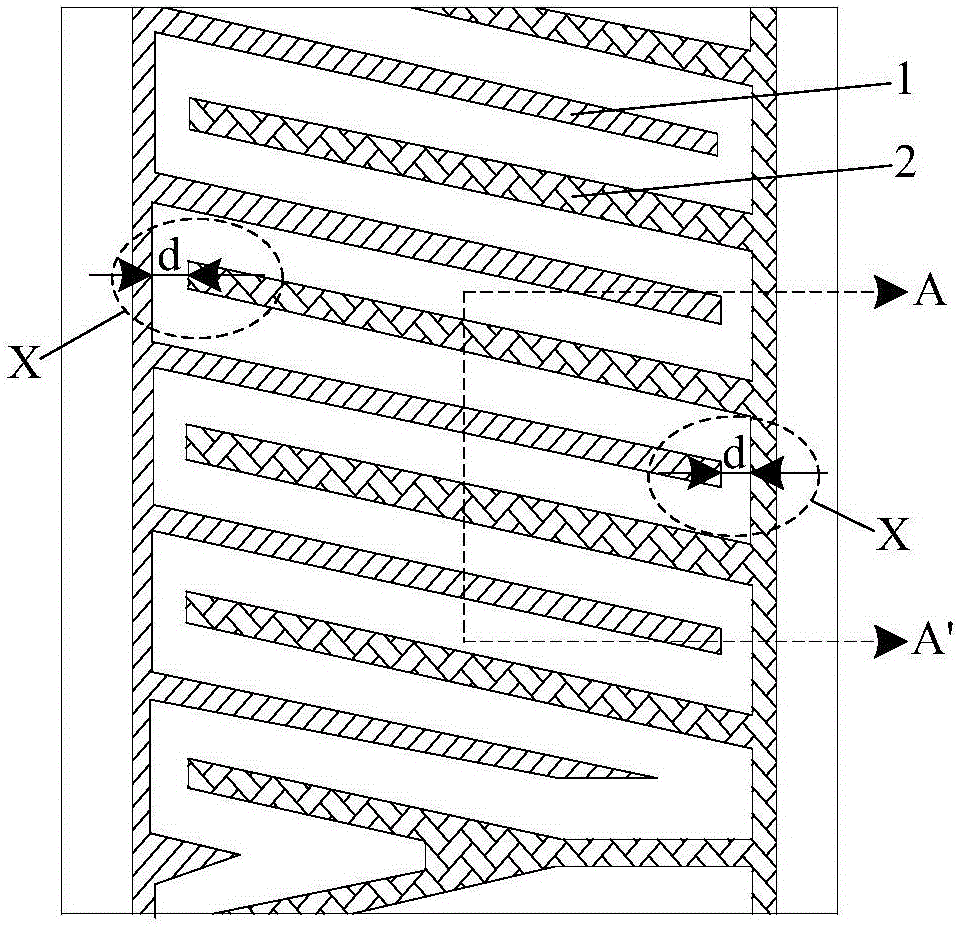
[0027] As mentioned in the background art, the array substrate using the comb electrode structure in the prior art has the problem of low light transmittance. The inventors of the present invention have found through research that one of the reasons for the above-mentioned problem is: as figure 1 with 2 As shown, since the pixel electrode 1 and the common electrode 2 are formed in the same patterning process in the prior art, the electrode material between the pixel electrode 1 and the common electrode 2 is etched to form the pattern of the pixel electrode 1 and the common electrode 2 In the process, limited by the process capability, there will be electrode material residue between the pixel electrode 1 and the common electrode 2. end, ie figure 1 The X shown in is especially serious. If the gap d between the pixel electrode 1 and the common electrode 2 at X is too small, there will be more electrode material remaining between the two at X, causing the two to be unable to ...

Embodiment 2

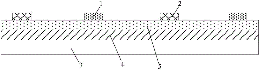
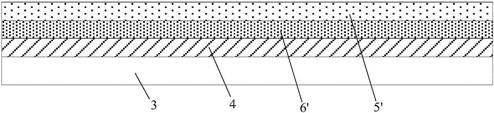
[0048] This embodiment provides an array substrate, such as Image 6 As shown, the array substrate includes: a base substrate 3, a first electrode 6 disposed on the base substrate 3, a passivation layer 5 covering the first electrode 6 and roughly the same shape as the first electrode 6, disposed on the substrate The second electrode 8 on the base substrate 3 . Wherein, an electric field can be formed between the first electrode 6 and the second electrode 8 , and the electric field may include a horizontal electric field parallel to the base substrate 3 for driving liquid crystal molecules to deflect.

[0049] In the above array substrate, since the passivation layer 5 and the first electrode 6 have approximately the same shape, the passivation layer 5 and the first electrode 6 can be formed in the same patterning process, and since the passivation layer 5 covers the first Therefore, the first electrode 6 and the second electrode 8 can be formed in different patterning proces...

Embodiment 3

[0059] This embodiment provides a display device, which includes the array substrate as described in the second embodiment. Since the gap between the first electrode and the second electrode in the array substrate described in the second embodiment can be set smaller, the light transmittance is higher, and the signal crosstalk between the first electrode and the second electrode is acceptable. Therefore, the display device including the array substrate also has the advantages of high light transmittance and signal crosstalk within an acceptable range.

[0060] It should be noted that the display device provided in this embodiment is preferably a liquid crystal display device, specifically any product with a display function such as a liquid crystal panel, a mobile phone, a tablet computer, a television, a monitor, a notebook computer, a digital photo frame, a navigator, etc. or parts.


PUM


Abstract

The invention provides an array substrate and manufacturing method thereof and display device, relates to the technical field of display, and can solve the problem of low light transmissivity when an array substrate of a comb-shaped electrode structure is adopted. The manufacturing method of the array substrate includes the steps of: forming a first conductive thin film and a passivation layer thin film on a lining substrate in sequence; adopting a one-time composition process, removing the passivation layer thin film and the first conductive thin film except a to-be-formed first electrode area, and forming a graph of a passivation layer and a graph of a first electrode; forming a second conductive thin film on the lining substrate having the graph of the passivation layer and the graph of the first electrode; and adopting the one-time picture composition process, removing the second conductive thin film except a to-be-form second electrode area, and forming a graph of a second electrode. The manufacturing method of the abovementioned array substrate is used for manufacturing the array substrate.

Description

technical field [0001] The present invention relates to the field of display technology, in particular to an array substrate, a manufacturing method thereof, and a display device. Background technique [0002] Liquid crystal display device is currently the most mainstream display device in the field of display technology. According to the different arrangement of liquid crystal molecules, liquid crystal display devices can be divided into TN (Twisted Nematic, twisted nematic) type, IPS (In-Plane Switching, in-plane switching) Type, VA (VerticalAlignment, vertical orientation) type and other types. Among them, the IPS type liquid crystal display device has the advantages of wide viewing angle, fast response speed, accurate color reproduction, etc., and has received extensive attention in the field. [0003] The array substrate of the IPS liquid crystal display device has various structures, and the manufacturing process of the array substrate of one structure requires four p...

Claims


Application Information

Patent Timeline
Patent Type & Authority Applications(China)
IPC IPC(8): H01L27/12G02F1/1362G02F1/1333H01L21/77
CPCG02F1/1333G02F1/1362H01L21/77H01L27/12G02F1/134309G02F1/134363G02F2201/124H01L27/124H01L27/1259G02F1/136295G02F1/13625G02F1/136227G02F1/136286G02F1/1368
Inventor 田允允张慧崔贤植
Owner BOE TECH GRP CO LTD
Why Eureka
Try Eureka