
Programmable electronic load for analog electronic technique teaching
An electronic load and analog electronic technology, applied in the field of electronics, can solve the problems of heavy workload and high cost
- Summary
- Abstract
- Description
- Claims
- Application Information
AI Technical Summary
Problems solved by technology
Method used
Image

Examples
Embodiment Construction
[0010] The present invention will be further described below in conjunction with the accompanying drawings.
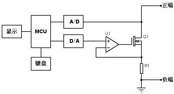
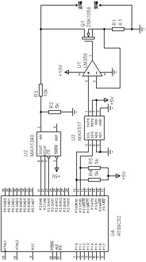
[0011] Such as figure 1 As shown, the program-controlled electronic load of the present invention includes a voltage-controlled current source unit, an A / D conversion unit, a D / A conversion unit, an MCU control unit, a keyboard unit, and a display unit; the voltage-controlled current source unit is composed of a high-power field effect Composed of tube Q1, current sampling resistor R1 and operational amplifier U1, the non-inverting input terminal of operational amplifier U1 is connected to the output terminal of the D / A conversion unit, and the inverting input terminal of operational amplifier U1 and one end of current sampling resistor R1 are connected to the large The source of the power FET Q1, the other end of the current sampling resistor R1 is used as the negative terminal of the electronic load and grounded, the output terminal of the operational amplifier U1 is...
PUM
 Abstract
Description
Claims
Application Information