Optical micro-structure and manufacturing method of optical micro-structure layer, light guide assembly and display device

An optical microstructure and light guide component technology, applied in optical components, light guides, optics, etc., can solve the problems of changing the phase distribution of holographic lenses, limiting the feasibility of mass production, product reliability, and defects, and avoiding changes in the phase distribution. , the effect of good mass production feasibility and product reliability

Active Publication Date: 2017-10-03
BOE TECH GRP CO LTD
View PDF6 Cites 12 Cited by
  • Summary
  • Abstract
  • Description
  • Claims
  • Application Information

AI Technical Summary

Problems solved by technology

[0003] However, in practical industrial applications, nanoimprinting technology has difficulties in preparing imprinting templates for large-scale products, and it is easy to cause defects when imprinting cross-scale microstructures. Issues such as changes in phase distribution, which limit mass production feasibility and product reliability

Method used


Image

  • Optical micro-structure and manufacturing method of optical micro-structure layer, light guide assembly and display device
  • Optical micro-structure and manufacturing method of optical micro-structure layer, light guide assembly and display device
  • Optical micro-structure and manufacturing method of optical micro-structure layer, light guide assembly and display device

Examples


Embodiment Construction

[0055] In order to enable those skilled in the art to better understand the technical solution of the present invention, the method for fabricating the optical microstructure, the light guide assembly and the display device provided by the present invention will be described in detail below with reference to the accompanying drawings.

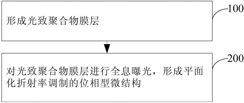
[0056] see figure 1 , the preparation method of the optical microstructure provided by the invention, it comprises:

[0057] 100, forming a photopolymer film layer;

[0058] 200. Perform holographic exposure on the photopolymer film layer to form a phase-type microstructure with planarized refractive index modulation.

[0059] The above-mentioned photopolymer film layer is a kind of transparent resin, which has the advantages of high photosensitivity, high resolution, high diffraction efficiency and high signal-to-noise ratio. The photopolymer film layer can change its internal refractive index after being exposed to form a refractive index m...


PUM


Abstract

The invention provides an optical micro-structure and a manufacturing method of an optical micro-structure layer, a light guide assembly and a display device. The manufacturing method comprises the steps of forming a photopolymer film layer, and performing holographic exposure on the photopolymer film layer to form a phase-type micro-structure with planar refractive index modulation. According to the manufacturing method of the optical micro-structure, a large-size product can be prepared; a cross-scale light ray micro-structure can be separated by sections; besides, the change of phase distribution in a hololens, caused by clinging or filling of film layers, can be avoided; and in addition, the mass producibility and the product reliability are high.

Description

technical field [0001] The invention relates to the field of display technology, in particular to an optical microstructure and a manufacturing method of an optical microstructure layer, a light guide component and a display device. Background technique [0002] For the preparation of complex and fine optical microstructures on large-scale products, nanoimprinting technology is generally recommended in the industry. The basic principle of nanoimprint technology is to use a template with nano-patterns to imprint and replicate nano-patterns in equal proportions on a substrate coated with polymer materials by mechanical force (high temperature, high pressure). Because the cost of optical lithography mask and optical imaging equipment is omitted, it has the economic advantages of low cost and high output. [0003] However, in practical industrial applications, nanoimprinting technology has difficulties in preparing imprinting templates for large-scale products, and it is easy t...

Claims


Application Information

Patent Timeline
Patent Type & Authority Applications(China)
IPC IPC(8): G02B5/18G02B6/00
CPCG02B5/1857G02B6/004G02B6/0065G02B6/0026G02B6/0016G02B6/0036G02B6/0073
Inventor 王维孟宪东谭纪风高健陈小川吕敬董学
Owner BOE TECH GRP CO LTD
Why Eureka
Try Eureka