Data processing device and method based on imaging box chip, chip and imaging box

A technology of a data processing device and an imaging box chip, applied in directions such as printing, can solve problems such as abnormality of data processing modules, and achieve the effect of improving practicability

Active Publication Date: 2017-11-03
APEX MICROELECTRONICS CO LTD
View PDF17 Cites 4 Cited by
  • Summary
  • Abstract
  • Description
  • Claims
  • Application Information

AI Technical Summary

Problems solved by technology

[0005] The invention provides a data processing device, method, chip and imaging box based on the imaging box chip, which solves the problem in the prior art that when the chip of the target imaging box participating in the communication is abnormal, if the data communication on the bus is not monitored, the It is difficult to judge whether the problem is caused by the abnormality of the data processing module inside the chip of the target imaging box according to the data on the bus

Method used


Image

  • Data processing device and method based on imaging box chip, chip and imaging box
  • Data processing device and method based on imaging box chip, chip and imaging box
  • Data processing device and method based on imaging box chip, chip and imaging box

Examples


Embodiment 1

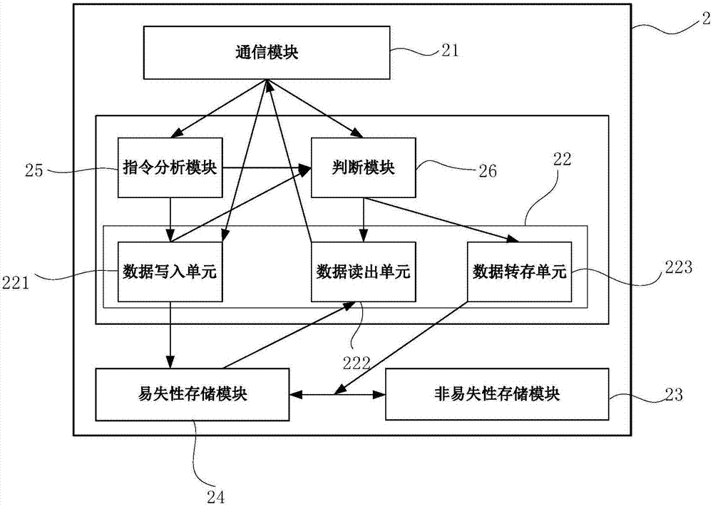
[0062] Continue to refer to the attached figure 1 , the types of access instructions include read instructions and write instructions, and the corresponding processing module 22 includes a data write unit 221 for write operations, a data read unit 222 for read operations, and a data load and dump operation Data transfer unit 223 .

[0063] When the output result of the instruction analysis module 25 is a write instruction, the processing module 22 is set to:

[0064] The data writing unit 221 is used to write the data content in the access instruction into the volatile storage module 24 when analyzing the access instruction as a write instruction;

[0065] Wherein, when the access instruction is a write instruction, the access instruction includes the data content to be written into the chip 2. In order to improve the efficiency of data processing, regardless of whether the target ID matches the ID of the chip, it is more preferable to directly write the The data content is ...

Embodiment 2

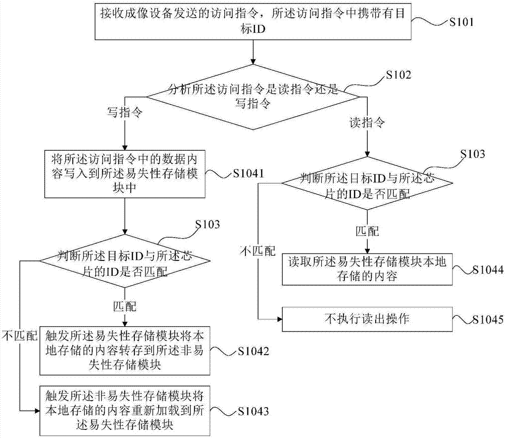
[0083] Continue to refer to the attached figure 1 The volatile storage module 24 of this embodiment is different from the volatile storage module 24 provided in Embodiment 1. The volatile storage module 24 in this embodiment is set to include: a data read-write area and a data recovery area, Among them, the data read-write area is used for data writing and reading, and the data recovery area is used for recovering data in the data read-write area; correspondingly:

[0084] When the output result of the instruction analysis module 25 is a write instruction, the processing module 22 is configured to include:

[0085] The data writing unit 221 is also used to write the data content in the access instruction into the data read-write area when analyzing the access instruction as a write instruction;

[0086] Wherein, when the data writing unit 221 analyzes the access command as a write command, it needs to write the data content in the access command into the data read / write area ...

Embodiment 3

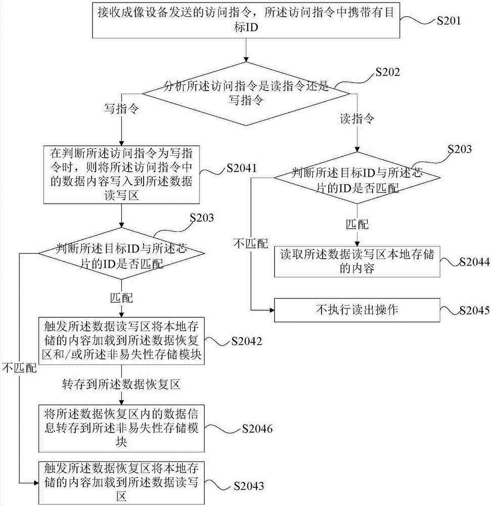
[0101] Continue to refer to the attachedfigure 1 , the volatile storage module 24 of this embodiment is different from the volatile storage module 24 provided in Embodiment 1 or Embodiment 2, and the volatile storage module 24 in this embodiment is set to include: a data writing area and Data readout area, wherein, the data write-in area is used to store the data to be written, and the data readout area is used to store the data to be read out; correspondingly:

[0102] When the output result of the instruction analysis module 25 is a write instruction, the processing module 22 is set to:

[0103] The data writing unit 221 is further configured to write the data content in the access instruction into the data writing area when analyzing that the access instruction is a write instruction.

[0104] When the output result of the command analysis module 25 is that the access command is a write command, it means that the imaging device has data content written into the chip 2 at th...


PUM


Abstract

The invention provides a data processing device and method based on an imaging box chip, the chip and an imaging box. The chip comprises a volatile storage module and a nonvolatile storage module connected with the volatile storage module. ID of the chip is stored in the nonvolatile storage module. The data processing device comprises a communication module, an instruction analysis module, a judgement module and a data writing unit, wherein the communication module is used for being connected to a bus of imaging equipment and receiving an access instruction sent by the imaging equipment, and the access instruction carries a target ID; the instruction analysis module is connected with the communication module and used for analyzing whether the access instruction is a reading instruction or a writing instruction; the judgement module is connected with the communication module and used for judging whether the target ID is matched with the ID of the chip; and the data writing unit is connected with the instruction analysis module, the judgement module and the volatile storage module and used for writing data contents in the access instruction into the volatile storage module if the access instruction is the writing instruction before whether the target ID and the ID of the chip is matched or not is judged.

Description

technical field [0001] The invention relates to the technical field of printing and imaging, in particular to a data processing device, method, chip and imaging box based on an imaging box chip. Background technique [0002] Imaging equipment, such as printers, copiers, and fax machines, is used to image information to be imaged on media such as paper through ink, toner, and other imaging materials. An imaging device generally includes an imaging device main body and an imaging cartridge, which is usually detachably installed in the imaging device main body. In order to mark the consumption or residual information of the imaging material in the imaging box, a chip is often arranged on the imaging box, and the chip is usually installed on the imaging box in a detachable manner. The chip is usually provided with a non-volatile memory module, which is used to store rewritable data such as the consumption or remaining amount of the imaging material, and other read-only data rel...

Claims


Application Information

Patent Timeline
Patent Type & Authority Applications(China)
IPC IPC(8): B41J2/175
CPCB41J2/17546
Inventor 李博康泽华
Owner APEX MICROELECTRONICS CO LTD
Why Eureka
Try Eureka