Pixel defining layer and manufacturing method thereof, display substrate, display panel

A technology for defining a pixel definition layer and a display substrate, which is applied in semiconductor/solid-state device manufacturing, semiconductor devices, electrical components, etc., and can solve problems such as the influence of film formation uniformity

Active Publication Date: 2020-07-07
BOE TECH GRP CO LTD
View PDF6 Cites 0 Cited by
  • Summary
  • Abstract
  • Description
  • Claims
  • Application Information

AI Technical Summary

Problems solved by technology

[0005] In order to solve the problem that the pixel-defining layer in the prior art can only suppress the climbing of the film layer close to the lyophobic layer to a certain extent, and the film-forming uniformity of the solution in the pixel area will still be affected, the embodiment of the present invention Provided are a pixel defining layer, a manufacturing method thereof, a display substrate, and a display panel

Method used


Image

  • Pixel defining layer and manufacturing method thereof, display substrate, display panel
  • Pixel defining layer and manufacturing method thereof, display substrate, display panel
  • Pixel defining layer and manufacturing method thereof, display substrate, display panel

Examples


Embodiment Construction

[0049] In order to make the object, technical solution and advantages of the present invention clearer, the implementation manner of the present invention will be further described in detail below in conjunction with the accompanying drawings.

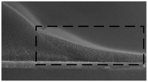
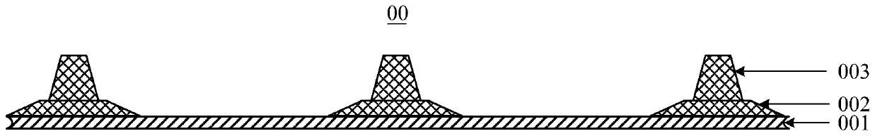
[0050]Compared with liquid crystal displays, OLED displays have the advantages of self-illumination, fast response, wide viewing angle, high brightness, bright colors and thinness. There are mainly two methods for manufacturing the film layer in organic electroluminescent devices: vacuum evaporation and solution process. Vacuum evaporation is suitable for the film formation of organic small molecule materials. It has the advantages of good film formation uniformity and relatively mature technology, and has been applied in mass production. The solution process includes methods such as spin coating, inkjet printing, and nozzle coating. Among them, inkjet printing technology is considered to be an important way to achieve mass production o...


PUM


Abstract

The invention discloses a pixel defining layer, a manufacturing method thereof, a display substrate and a display panel, and belongs to the field of display technology. The pixel defining layer includes: at least two sub-defining layers sequentially stacked on the base substrate; wherein, in every two sub-defining layers that are in contact with each other, the sub-defining layer far away from the base substrate is on the base substrate The first orthographic projection of is located within the second orthographic projection of the sub-defining layer close to the base substrate on the base substrate, and the edges of the first orthographic projection do not coincide with the edges of the second orthographic projection , and the surface of each sub-defining layer parallel to the substrate is lyophobic, and the side of each sub-defining layer is lyophilic. The invention suppresses the climbing of multiple film layers included in the organic light-emitting layer on the pixel defining layer, thereby effectively improving the film-forming uniformity of the solution in the pixel area. The invention is used for manufacturing OLED display panels.

Description

technical field [0001] The invention relates to the field of display technology, in particular to a pixel defining layer and a manufacturing method thereof, a display substrate, and a display panel. Background technique [0002] An organic light-emitting diode (English: Organic Light-Emitting Diode; abbreviation: OLED) display panel includes an anode, an organic light-emitting layer, and a cathode. Wherein, the organic light-emitting layer includes a hole injection layer, a hole transport layer, an organic light-emitting material layer, an electron transport layer, an electron injection layer, etc., and the organic light-emitting layer can be manufactured by inkjet printing technology. When using inkjet printing technology to manufacture an organic light-emitting layer, it is necessary to form a pixel defining layer on a glass substrate first, and then spray a solution that dissolves the material of the organic light-emitting layer onto the glass substrate on which the pixel...

Claims


Application Information

Patent Timeline
Patent Type & Authority Patents(China)
IPC IPC(8): H01L27/32H01L21/77
CPCH01L21/77H10K59/122H10K71/191H10K71/135H10K71/00
Inventor 胡春静
Owner BOE TECH GRP CO LTD
Why Eureka
Try Eureka