Array substrate and production thereof, driving method, display panel and display device

A technology of an array substrate and a driving method, which is applied in the field of display panels and can solve problems such as high driving voltage, power consumption, and multiple power consumption

Pending Publication Date: 2018-06-12
BOE TECH GRP CO LTD +1
View PDF7 Cites 4 Cited by
  • Summary
  • Abstract
  • Description
  • Claims
  • Application Information

AI Technical Summary

Problems solved by technology

Taking Notebook as an example, the driving voltage input by the data line or the pixel electrode voltage Vpixel is 0~8V, and the common electrode voltage Vcom is 4V. Considering the polarity inversion, the voltage difference between the pixe...

Method used


Image

  • Array substrate and production thereof, driving method, display panel and display device
  • Array substrate and production thereof, driving method, display panel and display device
  • Array substrate and production thereof, driving method, display panel and display device

Examples


Embodiment Construction

[0038] In order to make the above objects, features and advantages of the present invention more comprehensible, the present invention will be further described in detail below in conjunction with the accompanying drawings and specific embodiments.

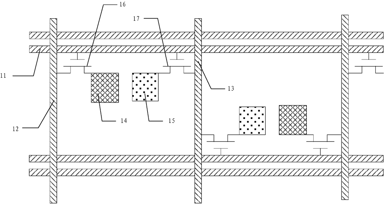
[0039] An embodiment of the present application provides an array substrate, referring to figure 1 , the array substrate may include: a plurality of pixel units divided by gate lines 11 and signal lines, wherein the signal lines include first signal lines 12 and second signal lines 13, and each pixel unit includes a pixel electrode 14 and a common electrode 15; the pixel unit includes a first thin film transistor 16 and a second thin film transistor 17, the gate of the first thin film transistor 16 is connected to the same gate line 11 as the gate of the second thin film transistor 17; the first thin film transistor 16 The first pole is connected to the first signal line 12 , the second pole is connected to the pixel electrode 14 ...


PUM


Abstract

The application provides an array substrate and production method thereof, a driving method, a display panel and a display device in order to reduce displaying power consumption; two thin-film transistors are arranged on a pixel unit to control charging for pixel electrodes and common electrodes, so that separate voltage adjustment is achieved for the pixel electrodes and the common electrodes; when a voltage difference between the pixel electrodes and the common electrodes is about to reach -4 to +4 V, their voltage adjusting ranges can be -2 to 2 V, namely driving voltage ranges of first andsecond signal lines can be -2 to 2 V. Compared with the prior art where driving voltage of data lines is 0-5 V, the array substrate and the production method thereof, the driving method, the displaypanel and the display device have the advantages that driving voltages on the first and second signal lines are greatly decreased and displaying energy consumption is further reduced.

Description

technical field [0001] The present invention relates to the technical field of display panels, in particular to an array substrate, a manufacturing method thereof, a driving method, a display panel and a display device. Background technique [0002] TFT-LCD (Thin Film Transistor-Liquid Crystal Display) is still the mainstream display product at present. With the popularity of smart phones and TVs, the market demand is increasing. In recent years, major panel manufacturers have been continuously devoting themselves to reducing the power consumption of TFT-LCD display products. [0003] In the process of driving and displaying the LCD, a voltage difference of 0-4V needs to be formed between the voltage of the pixel electrode and the voltage of the common electrode to drive the liquid crystal to deflect and then control the grayscale display. Taking Notebook as an example, the driving voltage input by the data line or the pixel electrode voltage Vpixel is 0~8V, and the common ...

Claims


Application Information

Patent Timeline
IPC IPC(8): G02F1/1362G02F1/1368G02F1/133H01L27/12H01L21/77
CPCG02F1/13306G02F1/136286G02F1/1368H01L27/124H01L27/1259
Inventor 汪锐李少茹马晓峰尚飞
Owner BOE TECH GRP CO LTD
Why Eureka
Try Eureka