Display method and display device

A display method and display panel technology, applied in static indicators, instruments, etc., can solve the problems of high switching frequency and high power consumption

Active Publication Date: 2018-12-18
BOE TECH GRP CO LTD +1
View PDF7 Cites 3 Cited by
  • Summary
  • Abstract
  • Description
  • Claims
  • Application Information

AI Technical Summary

Problems solved by technology

[0007] The present invention at least partly solves the problem of excessive power consumption in the existing display device due to the...

Method used


Image

  • Display method and display device
  • Display method and display device
  • Display method and display device

Examples


Embodiment 1

[0040] This embodiment provides a display method, which is applied to a display panel.

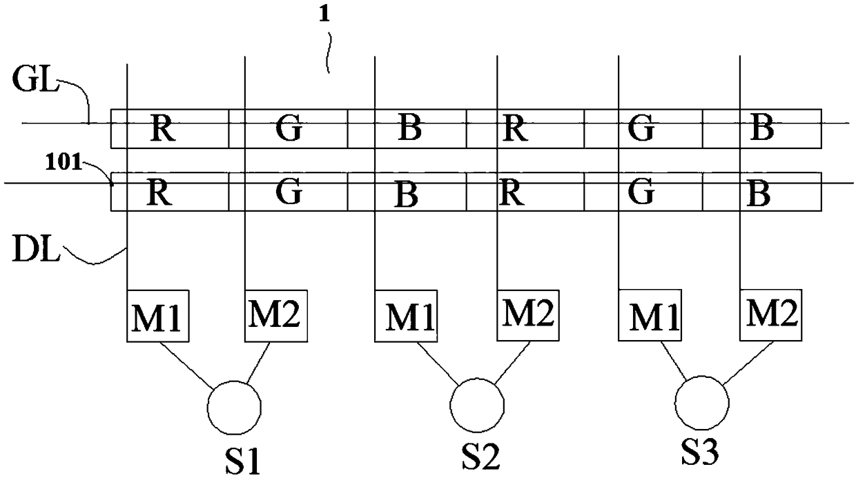
[0041] see figure 1 , the display panel 1 includes sub-pixels (such as red sub-pixel R, green sub-pixel G, blue sub-pixel B) distributed in an array, a plurality of data terminals (such as first data terminal S1, second data terminal S2, second data terminal Three data terminals S3), each data terminal is respectively connected to a plurality of storage units (such as the first storage unit M1, the second storage unit M2), each storage unit is connected to a data line DL, and is used to store the data voltage stored therein It is provided to the corresponding data line DL; in each row of sub-pixels, different data lines DL corresponding to the same data terminal are connected to different sub-pixels.

[0042] The sub-pixels may include light emitting diodes (organic light emitting diodes or micro light emitting diodes, etc.). That is, the display panel 1 may be an organic light emitting ...

Embodiment 2

[0060] This embodiment provides a display device to implement the display method provided in Embodiment 1.

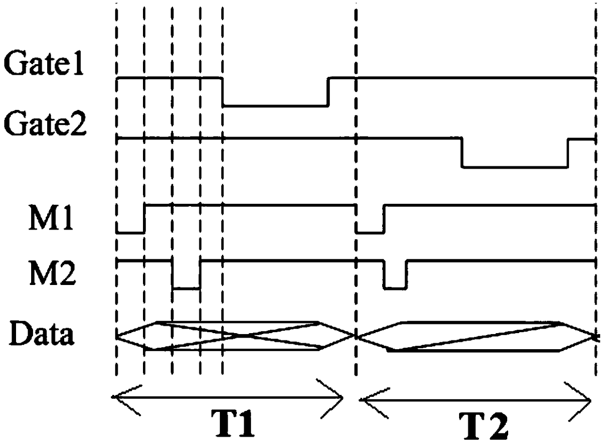
[0061] Such as figure 1 and 4 As shown, it includes a display panel 1 and a driving circuit 2 . The display panel 1 includes sub-pixels distributed in an array and a plurality of data terminals, each data terminal is respectively connected to a plurality of storage units, each storage unit is respectively connected to a data line DL, and is used to provide the data voltage stored therein to the corresponding In each row of sub-pixels, different data lines DL corresponding to the same data terminal are connected to different sub-pixels. Refer to the foregoing description for details.

[0062] The driving circuit 2 is used for writing data voltages to a row of sub-pixels according to the aforementioned display method in each row period among the plurality of row periods.

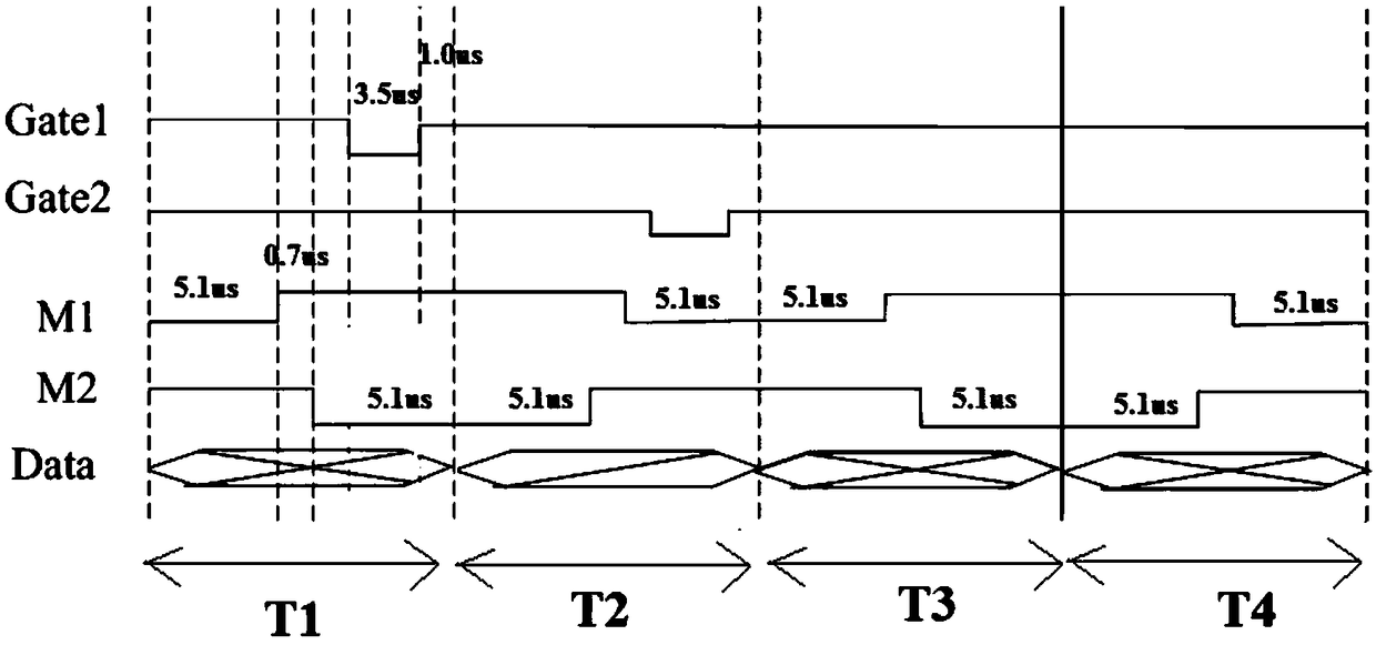
[0063] Specifically, the drive circuit 2 includes a storage unit control module 21, the storage ...


PUM


Abstract

The invention provides a display method and a display device, and belongs to the display technical field; switch elements of memory units in a display panel of an existing display device are frequently opened/closed, thus causing large power consumption; the display method and display device can at least partially solve said problems. The display method comprises a plurality of line periods, and data voltage is written in a line of sub-pixels in each line period, wherein each memory unit connected with the same data end can receive and store the data voltage from the data end in turns in eachline period, and each memory unit only receives the data voltage for once; in at least two adjacent line periods, at least one memory unit receives the data voltage in the rear stage of the previous line period and the front stage of the following line period.

Description

technical field [0001] The invention belongs to the field of display technology, and in particular relates to a display method and a display device. Background technique [0002] A display panel (such as a liquid crystal display panel, an OLED display panel, a micro light-emitting diode display panel, etc.) usually includes a plurality of sub-pixels distributed in an array. A plurality of data terminals are set in the display panel, and the driving circuit (specifically, for example, a source driver chip, also called Source IC) provides data voltages to these data terminals, and the driving circuit (specifically, for example, a timing driver chip, also called T-con IC) controls each row of sub-pixels to receive corresponding data voltages sequentially. The sub-pixels emit light according to the magnitude of the data voltage. [0003] When the density of sub-pixels in the display panel is too high, or the PPI is too high, this results in limited space for setting data termi...

Claims


Application Information

Patent Timeline
IPC IPC(8): G09G3/3291G09G3/36
CPCG09G3/3291G09G3/3696
Inventor 喻勇申丽霞张昌兰传艳
Owner BOE TECH GRP CO LTD
Why Eureka
Try Eureka