

Dual-band terahertz wave absorber of graphene metasurface
A wave absorber and metasurface technology, applied in the terahertz field, can solve problems such as large structure size, low absorption rate, and complex structure, and achieve good absorption effect, simple structure, and easy realization
- Summary
- Abstract
- Description
- Claims
- Application Information
AI Technical Summary
Problems solved by technology
Method used
Image

Examples
Embodiment Construction
[0021] The present invention will be further described in detail below in conjunction with the accompanying drawings and specific embodiments.
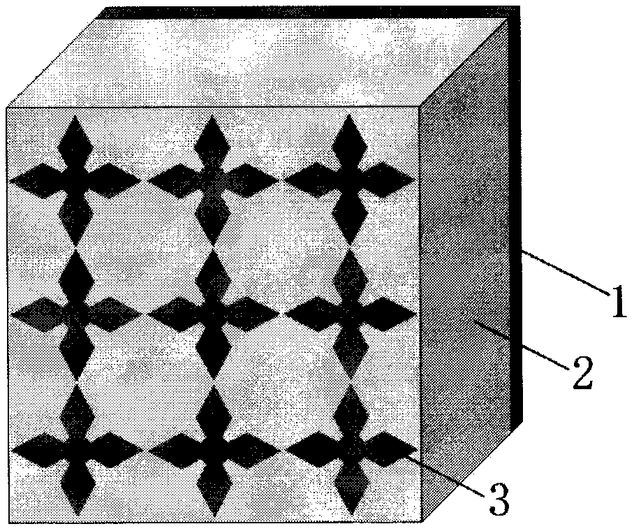
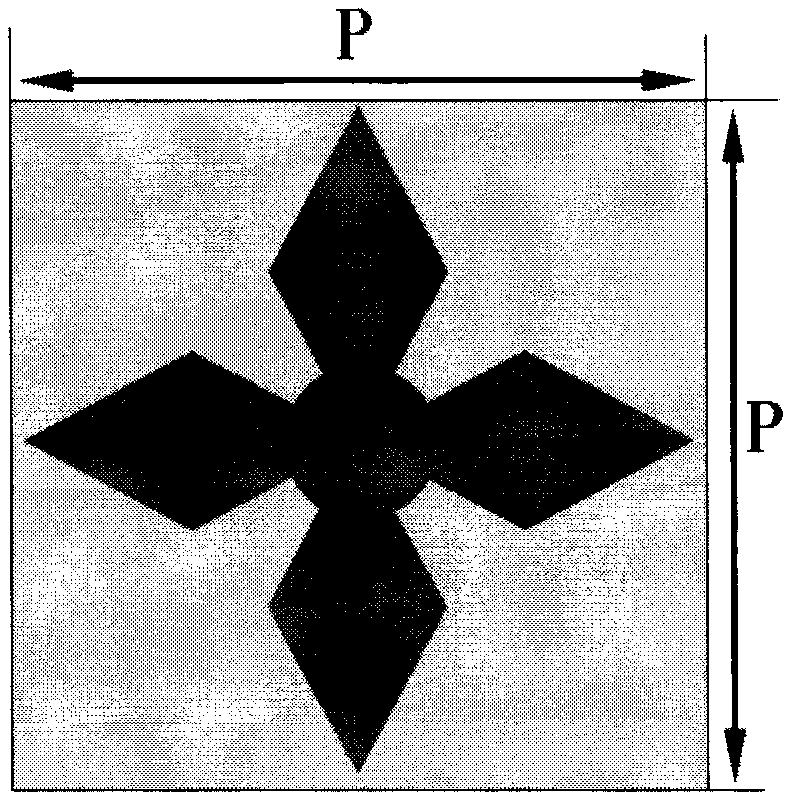
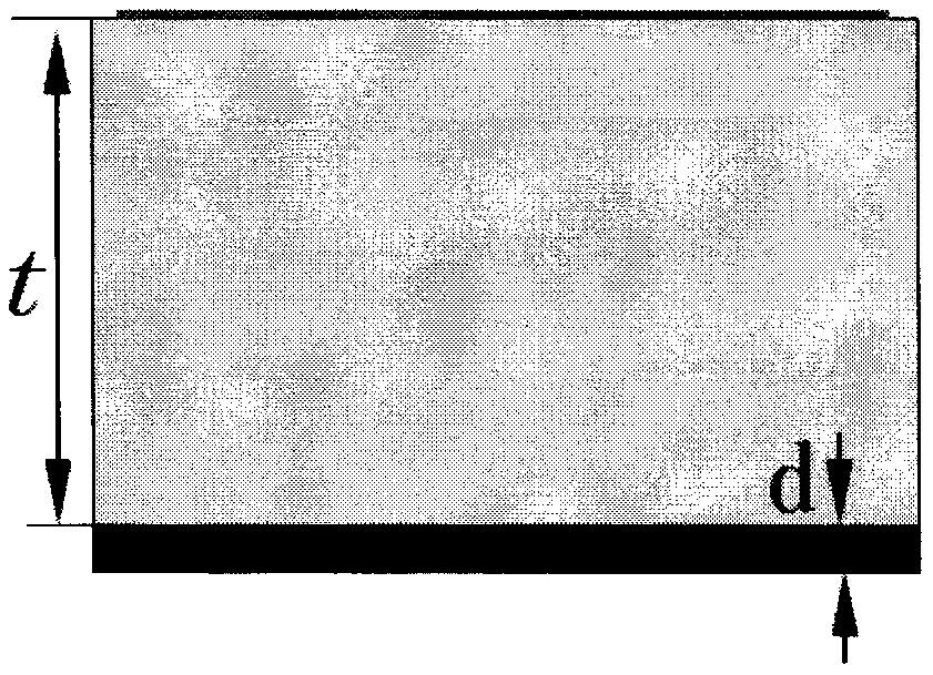
[0022] Such as Figure 1~3 As shown, a graphene metasurface dual-band terahertz absorber includes multiple absorbing units arranged continuously along the plane. The absorber unit is composed of the bottom metal film (1), the middle dielectric layer (2) and the top graphene film (3) arranged in sequence from bottom to top, the bottom metal film (1), the middle dielectric layer (2) and the top layer The graphene films (3) are attached to each other. The bottom metal film (1) is an all-metal film, and the top graphene film (3) is a patterned single-layer graphene, the geometric center of the patterned single-layer graphene, the geometric center of the intermediate dielectric layer (2) And the geometric center of the underlying metal film (1) is on a straight line.
[0023] When multiple absorbing units are arranged continuously along...
PUM
| Property | Measurement | Unit |
|---|---|---|
| Thickness | aaaaa | aaaaa |
| Thickness | aaaaa | aaaaa |
| Radius | aaaaa | aaaaa |
Abstract
Description
Claims
Application Information