An organic compound and its application in organic electronic devices

A technology of organic electronic devices and organic compounds, which is applied in the field of organic electroluminescence, can solve the problems of device performance and life expectancy, and achieve the effects of improving electroluminescence efficiency and device life, close stacking, and effective transmission effect

Active Publication Date: 2022-04-29
广州追光科技有限公司
View PDF42 Cites 0 Cited by
  • Summary
  • Abstract
  • Description
  • Claims
  • Application Information

AI Technical Summary

Problems solved by technology

However, the obtained device performance and lifetime still need to be improved

Method used


Image

  • An organic compound and its application in organic electronic devices
  • An organic compound and its application in organic electronic devices
  • An organic compound and its application in organic electronic devices

Examples


preparation example Construction

[0099] The preparation method as described above is characterized in that the thickness of the formed functional layer is 5nm-1000nm.

[0100] The invention further relates to an organic electronic device comprising at least one organic compound according to the invention, or at least one functional layer, which is produced using a composition according to the invention. Generally, such an organic electronic device at least comprises a cathode, an anode and a functional layer between the cathode and the anode, wherein the functional layer contains at least one organic compound as mentioned above.

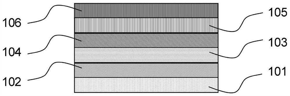
[0101] In a more preferred embodiment, the above-mentioned organic electronic device is an electroluminescent device, especially an OLED (such as figure 1 shown), which includes a substrate (101), an anode (102), at least one light-emitting layer (104), and a cathode (106).

[0102] OLEDs can also contain other functional layers such as hole injection layer (HIL) or hole transport...

Synthetic example 1

[0107] Synthesis Example 1: Synthesis of Compound 1

[0108]

[0109] Materials 1-1 (6.56g, 20mmol), 1-2 (5.3g, 20mmol), Pd(dba) 2 (0.345g, 0.6mmol), sodium tert-butoxide (5.76g, 60mmol) and tri-tert-butylphosphine (plasmid ratio 10%, 3.5ml) were placed in a 1000ml two-necked flask, anhydrous toluene 100mL was added under nitrogen protection, and 90 Celsius, and stir overnight. Cooled to room temperature, washed with water, dried, and purified by column chromatography to obtain compound 1 (7.8 g, 70%).

Synthetic example 2

[0110] Synthesis Example 2: Synthesis of Compound 2

[0111]

[0112] The raw material 2-1 (6.56g, 20mmol), 2-2 (6.8g, 20mmol), Pd (dba) 2 (0.345g, 0.6mmol), sodium tert-butoxide (5.76g, 60mmol) and tri-tert-butylphosphine (plasmid ratio 10%, 3.5ml) were placed in a 1000ml two-necked flask, anhydrous toluene 100mL was added under nitrogen protection, and 90 Celsius, and stir overnight. Cooled to room temperature, washed with water, dried, and purified by column chromatography to obtain compound 2 (8.9 g, 70%).


PUM

PropertyMeasurementUnit
boiling pointaaaaaaaaaa
thicknessaaaaaaaaaa

Abstract

The invention discloses an organic compound and its application in organic electronic devices, especially in organic electroluminescent diodes. The invention also discloses an organic electronic device comprising the organic compound according to the invention, especially an organic electroluminescence diode, and its application in display and lighting technology. The invention further discloses an organic electronic device prepared by using the composition according to the invention, and a preparation method. Through device structure optimization, better device performance can be achieved, especially high-performance OLED devices, which provide better material and preparation technology options for full-color display and lighting applications.

Description

technical field [0001] The invention relates to the technical field of organic electroluminescence, in particular to an organic compound, mixture and composition, and its application in the field of organic electronic devices, especially electroluminescent devices. Background technique [0002] Organic light-emitting diodes (OLEDs) have excellent properties such as light weight, active light emission, wide viewing angle, high contrast, high luminous efficiency, low energy consumption, easy fabrication of flexible and large-size panels, and are regarded by the industry as the most promising next-generation display technology . To obtain high-performance organic light-emitting diodes, the host material is the key. At present, OLED light-emitting devices are generally prepared by using a single-host material with a luminous body, but the single-host material will cause different carrier transfer rates, resulting in serious device efficiency roll-off (Roll-off) under high brigh...

Claims


Application Information

Patent Timeline
Patent Type & Authority Patents(China)
IPC IPC(8): C07D487/22C07D519/00C07D487/16C09K11/06H01L51/30H01L51/46H01L51/54
CPCC07D487/22C07D519/00C07D487/16C09K11/06C09K2211/1011C09K2211/1059C09K2211/1074C09K2211/1044C09K2211/1088C09K2211/1092C09K2211/1048C09K2211/1051H10K85/615H10K85/626H10K85/654H10K85/657H10K85/6576H10K85/6572H10K85/6574H10K10/46H10K30/00H10K50/11Y02E10/549
Inventor 杨曦
Owner 广州追光科技有限公司
Why Eureka
Try Eureka