Display panel

A technology of display panel and display area, applied in optics, instruments, electrical and digital data processing, etc., can solve the problems of inaccurate test values, difficult to test the operating parameters of the touch layer, affecting the quality judgment of the display panel, etc.

Active Publication Date: 2020-10-20
WUHAN CHINA STAR OPTOELECTRONICS TECH CO LTD
View PDF10 Cites 2 Cited by
  • Summary
  • Abstract
  • Description
  • Claims
  • Application Information

AI Technical Summary

Problems solved by technology

[0005] The invention provides a display panel, which can solve the technical problem that it is not easy to test the operating parameters of the touch layer in the low-temperature polysilicon display panel in the prior art, and the test value is prone to be inaccurate, which greatly affects the quality judgment of the display panel.

Method used


Image

  • Display panel
  • Display panel
  • Display panel

Examples


Embodiment Construction

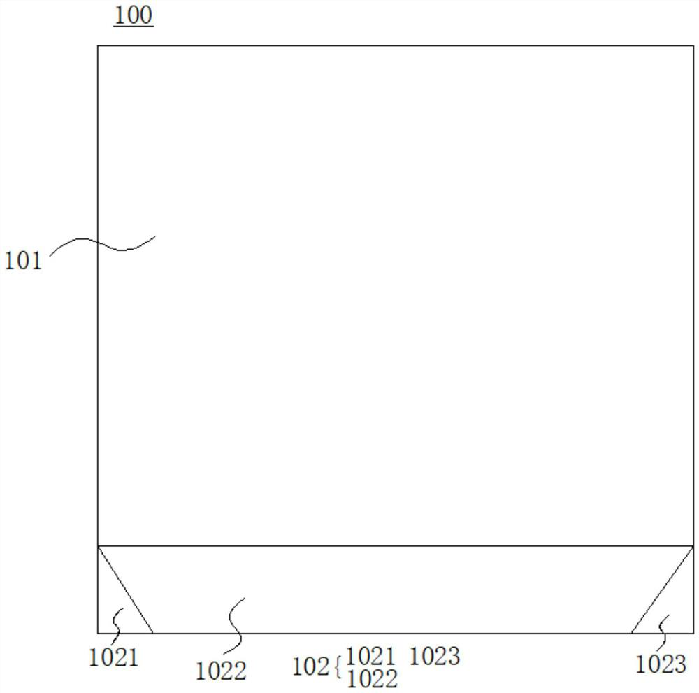
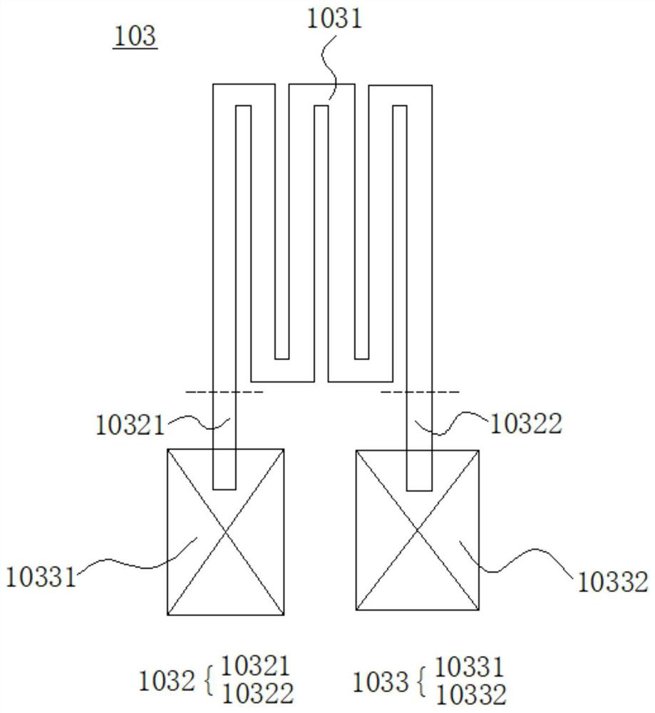
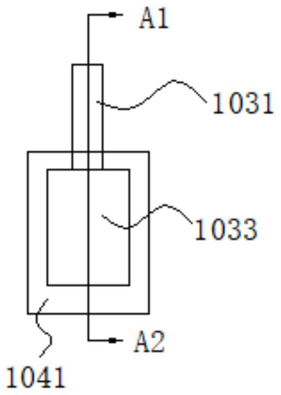
[0023] The following descriptions of the various embodiments refer to the accompanying drawings to illustrate specific embodiments in which the invention may be practiced. The directional terms mentioned in the present invention, such as [top], [bottom], [front], [back], [left], [right], [inside], [outside], [side], etc., are only for reference The orientation of the attached schema. Therefore, the directional terms used are used to illustrate and understand the present invention, but not to limit the present invention. In the figure, units with similar structures are indicated by the same reference numerals, and the dotted lines in the figure indicate that they do not exist in the structure, and only illustrate the shape and position of the structure.

[0024] The present invention aims at the technical problem that it is not easy to test the operating parameters of the touch layer in the low-temperature polysilicon display panel in the prior art, and the test value is prone...


PUM

PropertyMeasurementUnit
thicknessaaaaaaaaaa

Abstract

The invention provides a display panel. The display panel is characterized in that a test module is arranged in a non-display area of the display panel, and the test module at least comprises a test terminal, a test circuit and a test lead for connecting the test terminal and the test circuit, wherein an etching protection layer is formed on a surface of the test terminal, the etching protection layer is positioned between the driving electrode layer and the induction electrode layer of the touch layer, the test terminal is a part, extending to the non-display area, of the induction electrodelayer, the extended part is electrically connected with the etching protection layer, the overlapping area of the test terminals is increased, and the bending angle of a touch electrode in the touch layer is reduced. The display panel is advantaged in that stability of the test lead is improved, reliability and effectiveness of the test of the touch layer of the display panel are improved, and thetest module can be directly measured under the condition that the display panel is not damaged when a user is abnormal in use, so abnormality is analyzed, and maintenance cost of the display panel isreduced.

Description

technical field [0001] The present invention relates to the field of display technology, in particular to a display panel. Background technique [0002] At present, the integrated touch display panel mainly includes two types: the on-cell type in which the touch sensor is arranged between the polarizer of the display panel and the color filter substrate; and the on-cell type in which the touch sensor is embedded Embedded into the pixel structure of the display panel (In-Cell). [0003] Electrical testing in the manufacture of in-cell low-temperature polysilicon touch display panels is often a destructive test, which cannot be tested directly with the product circuit. It is necessary to extend the lead wires from the touch layer in the display panel, and then use probes to measure the lead wires in the test circuit. Voltage voltage, current, or resistance value, use these voltage, current, or resistance parameters to judge whether the LCD panel is operating normally, because...

Claims


Application Information

Patent Timeline
Patent Type & Authority Applications(China)
IPC IPC(8): G06F3/041G02F1/13G02F1/1333G02F1/1343
CPCG06F3/0412G06F3/04164G02F1/1309G02F1/13338G02F1/134309
Inventor 陈辰
Owner WUHAN CHINA STAR OPTOELECTRONICS TECH CO LTD
Why Eureka
Try Eureka