Circuit board design data processing method and device, electronic equipment and storage medium

A data processing and circuit board technology, applied in the direction of electrical digital data processing, CAD circuit design, special data processing applications, etc., can solve problems such as adverse effects of welding process

Inactive Publication Date: 2021-03-16
上海柏楚数控科技有限公司
View PDF7 Cites 0 Cited by
  • Summary
  • Abstract
  • Description
  • Claims
  • Application Information

AI Technical Summary

Problems solved by technology

[0004] The present invention provides a data processing method, device, electronic equipment and storage medium for circuit board design to solve the problem that when the marking points are placed too close to the edge of the board, it will adversely affect the welding process after the design.

Method used


Image

  • Circuit board design data processing method and device, electronic equipment and storage medium
  • Circuit board design data processing method and device, electronic equipment and storage medium
  • Circuit board design data processing method and device, electronic equipment and storage medium

Examples


Embodiment Construction

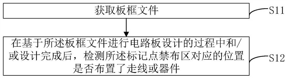
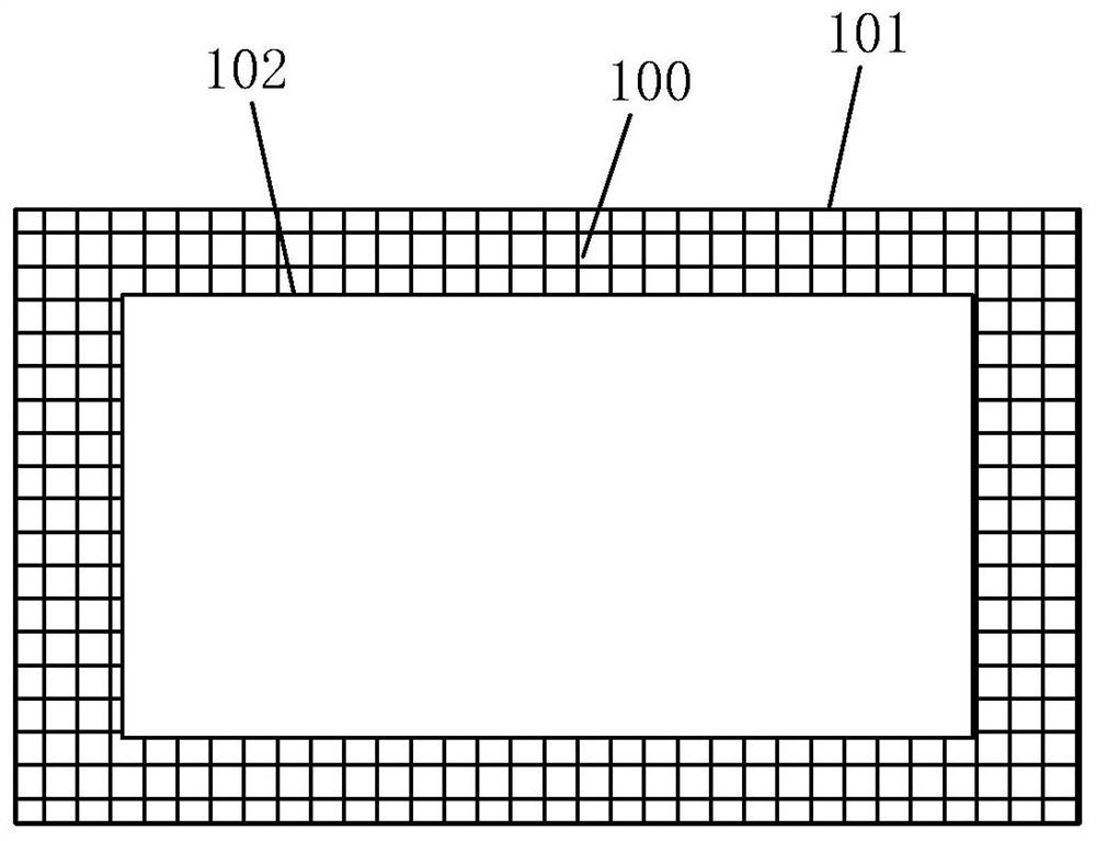
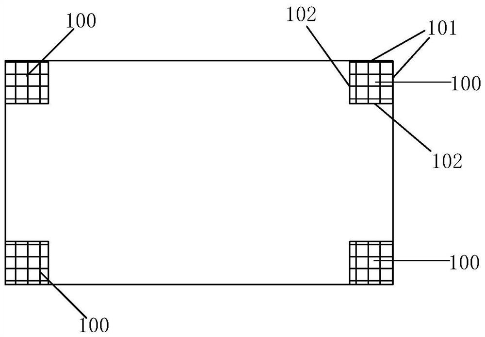
[0045] The technical solutions in the embodiments of the present invention will be clearly and completely described below in conjunction with the accompanying drawings in the embodiments of the present invention. Obviously, the described embodiments are only some of the embodiments of the present invention, not all of them. Based on the embodiments of the present invention, all other embodiments obtained by persons of ordinary skill in the art without making creative efforts belong to the protection scope of the present invention.

[0046] The terms "first", "second", "third", "fourth", etc. (if any) in the description and claims of the present invention and the above drawings are used to distinguish similar objects and not necessarily Describe a specific order or sequence. It is to be understood that the data so used are interchangeable under appropriate circumstances such that the embodiments of the invention described herein can be practiced in sequences other than those il...


PUM


Abstract

The invention provides a circuit board design data processing method and device, electronic equipment and a storage medium, and the method comprises the steps of obtaining a board frame file; in the board frame file, setting a marking point distribution forbidding area in the adjacent range of the edge of the circuit board; and in the process of designing the circuit board based on the board framefile and / or after the design is completed, detecting whether a wire or a device is arranged at a position corresponding to the marking point forbidden area.

Description

technical field [0001] The present invention relates to the field of PCB board design, in particular to a data processing method, device, electronic equipment and storage medium for circuit board design. Background technique [0002] Marking points, which can also be understood as optical positioning points, can also be described as Mark points. During the manufacturing process of circuit boards (or PCB boards, where the PCB is specifically Printed Circuit Board), the marking points can be used for solder paste printing and component placement. Optical positioning of device patches provides a common measurable point for all steps in the assembly process, which enables each device used in assembly to precisely position the circuit pattern. [0003] During the design process of the circuit board, the placement of the marking point has its specific specifications, for example, it cannot be placed too close to the edge of the board. If the marking points fail to meet the specif...

Claims


Application Information

Patent Timeline
Patent Type & Authority Applications(China)
IPC IPC(8): G06F30/394G06F30/398G06F115/12
CPCG06F30/394G06F30/398G06F2115/12
Inventor 卢琳孟丽芳徐沙沙于平平程朱贝
Owner 上海柏楚数控科技有限公司
Why Eureka
Try Eureka