
Optical coupling lens with circuit interfaces and assembly process of optical coupling lens
A circuit interface and assembly process technology, applied in the field of optical coupling lens and its assembly process, can solve problems such as single function, and achieve the effect of enriching functions
- Summary
- Abstract
- Description
- Claims
- Application Information
AI Technical Summary
Problems solved by technology
Method used
Image

Examples
Embodiment Construction
[0021] The specific implementation manners of the present invention will be further described in detail below in conjunction with the accompanying drawings and embodiments. The following examples are used to illustrate the present invention, but are not intended to limit the scope of the present invention.
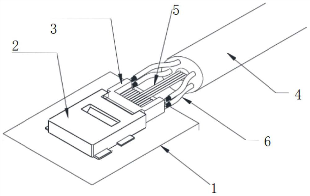
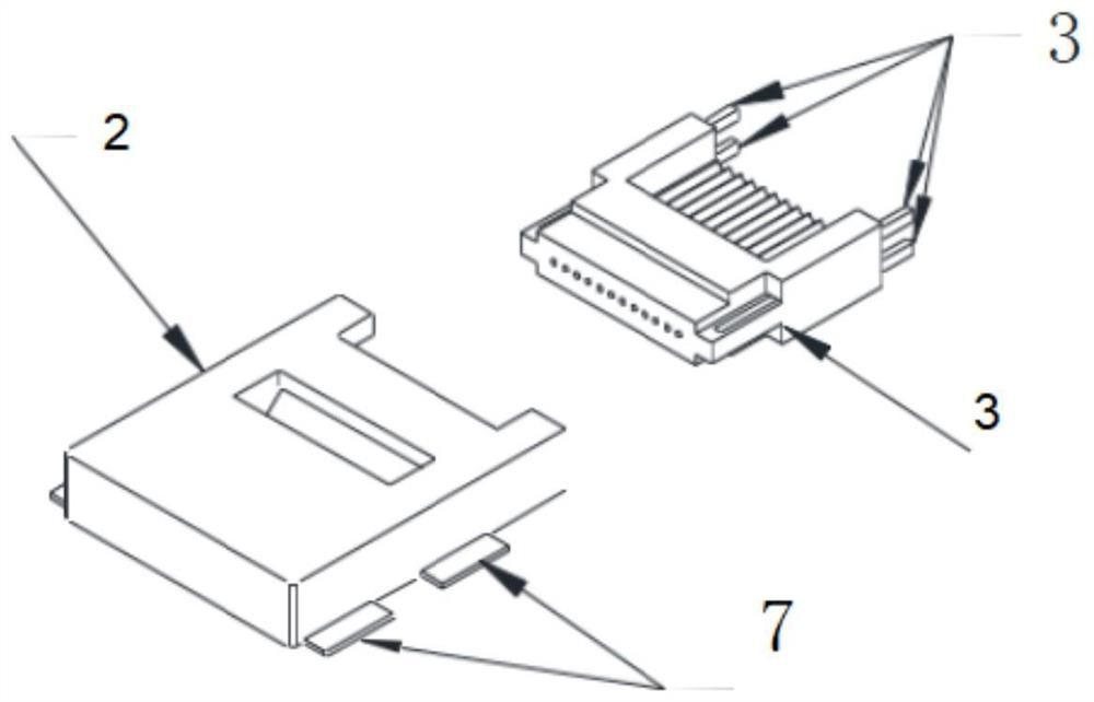
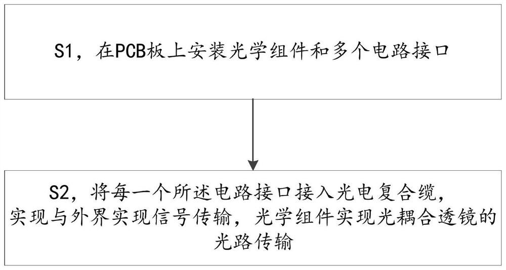
[0022] figure 1 Provided for the present invention is an optical coupling lens with a circuit interface, the optical coupling lens mainly includes a PCB board 1, an optical component and a plurality of circuit interfaces are installed on the PCB board 1, each of the circuit interfaces passes through a photoelectric composite cable 4 The electrical signal transmission is realized with the outside world, and the light guide channel of the optical component realizes the optical path transmission of the optical coupling lens.
[0023] It can be understood that, based on the defects in the background technology and as a requirement, the embodiment of the present invention prov...
PUM
 Abstract
Description
Claims
Application Information