

Packaging structure, printed circuit board and electronic equipment
A technology of packaging structure and electronic components, applied in the direction of printed circuit, printed circuit, printed circuit components, etc., can solve the problems of impedance discontinuity, achieve the effect of improving impedance continuity, increasing impedance, and improving signal transmission effect
- Summary
- Abstract
- Description
- Claims
- Application Information
AI Technical Summary
Problems solved by technology
Method used
Image

Examples
Embodiment 1
[0041] The pad assembly provided by Embodiment 1 of the present invention includes a conductive body in a strip structure.
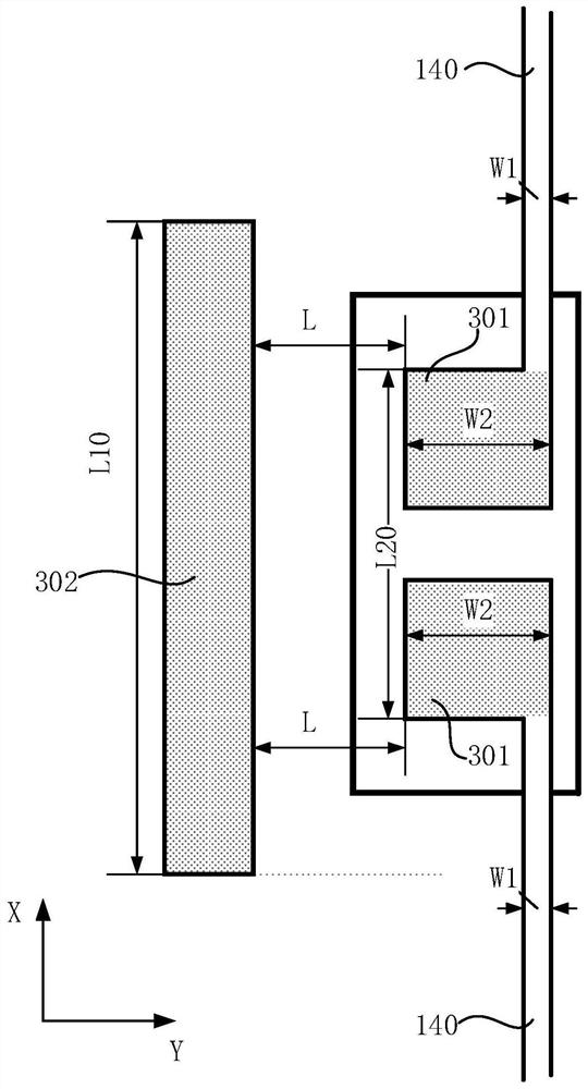
[0042] Optionally, as in image 3 As shown, the conductive body 302 has a strip-shaped structure, and the extension direction of the conductive body 302 is parallel to the extension direction of the signal line 140; in the direction X parallel to the extension direction of the signal line 140, the length L10 of the conductive body 302 is greater than or equal to the length L10 of the pad body 301 The length L20.
[0043] In this example, if image 3 As shown, the extension direction parallel to the signal line 140 is defined as the X direction, and the direction perpendicular to the signal line 140 is the Y direction. In the Y direction, the extension direction of the conductive body 302 is parallel to the X direction, and the pad body 301 has a rectangular structure. , the signal line 140 is connected to a vertex of the pad body 301 , and the edge of ...
Embodiment 2
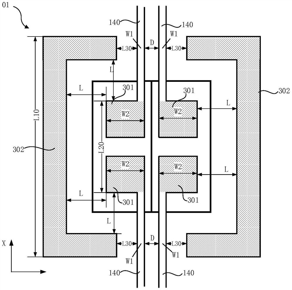
[0046] The pad assembly provided by Embodiment 2 of the present invention includes a conductive body in a semi-enclosed structure.
[0047] Optionally, as in figure 2 and 4 As shown, the conductive body 302 has a semi-enclosed structure, and the conductive body 302 has a first conductive portion 3021 parallel to the extending direction X of the signal line 140 and a second conductive portion 3022 perpendicular to the extending direction of the signal line 140; In the X direction of the extension direction of the signal line 140, the length L10 of the conductive body 302 is greater than or equal to the length L20 of the pad body 301; A distance threshold is set, wherein the minimum distance L30 between the conductive body 302 and the signal line 140 is the distance between the second conductive portion 3022 and the signal line 140 .
[0048] Specifically, such as figure 2 and 4 As shown, the extension direction parallel to the signal line 140 is defined as the X direction...
PUM
| Property | Measurement | Unit |
|---|---|---|
| thickness | aaaaa | aaaaa |
Abstract
Description
Claims
Application Information