Radiation detector

A radiation detector and detector technology, applied in the field of radiation detectors, can solve the problem of spectral sensitivity distribution difference matching and the like

Active Publication Date: 2007-03-28
OSRAM OPTO SEMICON GMBH & CO OHG
View PDF0 Cites 5 Cited by
  • Summary
  • Abstract
  • Description
  • Claims
  • Application Information

AI Technical Summary

Problems solved by technology

[0005] Applying such a silicon photodiode as a detector with a spectral sensitivity distribution adapted to the bright human eye - which has a sensitivity maximum at about 555 nm - requires additional overhead, since the wavelengths of the sensitivity maxima differ significantly from each other, and The two spectral sensitivity distributions are therefore poorly matched to each other

Method used


Image

  • Radiation detector
  • Radiation detector
  • Radiation detector

Examples


Embodiment Construction

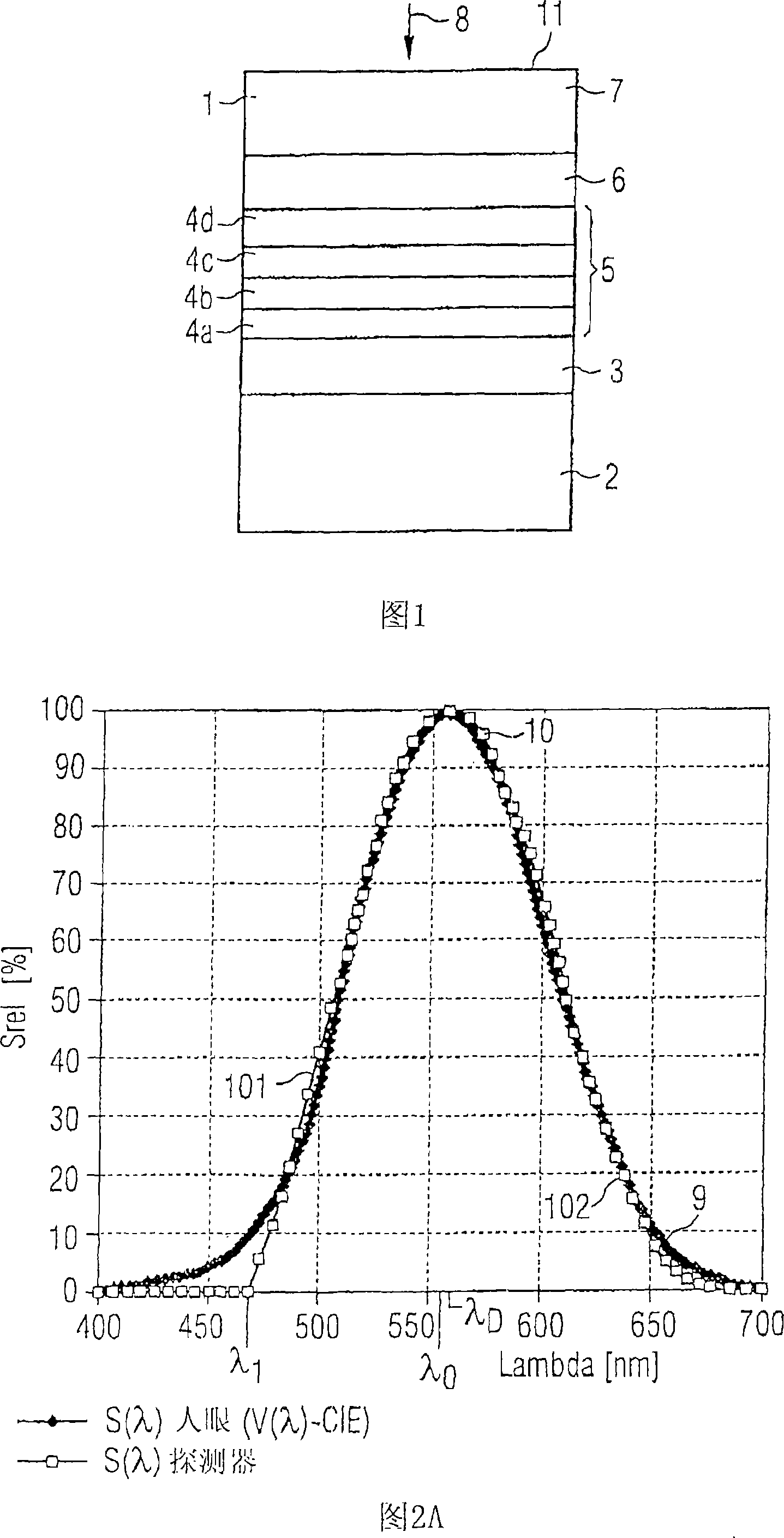
[0064] A first exemplary embodiment of a radiation detector according to the invention is shown in FIG. 1 with the aid of a schematic sectional illustration.

[0065]The semiconductor body 1 is arranged on a carrier 2 . On the carrier 2 side, an n-conducting layer 3 is arranged in the semiconductor body, followed by functional layers 4a, 4b, 4c and 4d of different band gaps and / or thicknesses, which essentially form the active layers of the semiconductor body. zone 5, and is used for detector signal generation. Preferably, every two arbitrary functional layers have different band gaps and thicknesses. A p-conducting layer 6 is arranged downstream of the functional layer, and a filter layer structure comprising a filter layer 7 follows. Preferably, the semiconductor body is formed monolithically with n- and p-conducting layers, filter layers and functional layers. Particularly preferably, the carrier is provided by a growth substrate of the semiconductor body. The semicondu...


PUM


Abstract

A radiation detector is disclosed, for the detection of radiation (8), with a given spectral sensitivity distribution (9), which has a maximum at a given wavelength lambdao, comprising a semiconductor body (1) with an active region (5), provided for detector signal generation and for the incident radiation. In one embodiment, the active region (5) comprises a number of functional layers (4a, 4b, 4c, 4d), with differing band gaps and / or thicknesses and embodied such that said layers (4a, 4b, 4c, 4d) at least partly absorb radiation at a wavelength greater than lambdao. In a further embodiment, a filter layer structure (70) is arranged after the active region, comprising at least one filter layer (7, 7a, 7b, 7c). The filter layer structure determines the short wave side (101) of the detector sensitivity (10), according to the given spectral sensitivity distribution (9), by means of absorption of wavelengths less than lambdao. A radiation detector for the detection of radiation (8), according to the spectral sensitivity distribution (9) of the human eye is also disclosed. The semiconductor body can be monolithically integrated.

Description

technical field [0001] The invention relates to a radiation detector for detecting radiation according to a predetermined spectral sensitivity distribution, wherein the sensitivity distribution is at a predetermined wavelength λ 0 There is a maximum at , the radiation detector comprising a semiconductor body having an active region for detector signal generation and for radiation reception. In particular, the invention relates to a radiation detector for detecting radiation according to a predetermined spectral sensitivity distribution of the human eye. Background technique [0002] In order to be at a predetermined wavelength λ 0 To detect radiation at a predetermined spectral sensitivity distribution with a maximum value, radiation detectors with specially adapted external filter arrangements, such as interference filters or monochromators, are often used. Such detectors are distinguished by a good match to a predetermined spectral sensitivity distribution, but are in mo...

Claims


Application Information

Patent Timeline
Patent Type & Authority Applications(China)
IPC IPC(8): H01L31/0216H01L31/068
CPCH01L31/02162H01L31/035236H01L31/03046Y02E10/544H01L31/0296H01L31/1035B82Y20/00Y02E10/547H01L31/115
Inventor 阿恩特·耶格彼得·施陶斯赖纳·温迪施
Owner OSRAM OPTO SEMICON GMBH & CO OHG
Why Eureka
Try Eureka