Apparatus and method for manufacturing liquid crystal display devices

a liquid crystal display and apparatus technology, applied in the manufacture of electric discharge tubes/lamps, printers, instruments, etc., can solve the problems of high probability of damage to the substrate(s) during the loading/unloading process, and the prior art substrate assembly device is problemati

Inactive Publication Date: 2005-01-27
AVACO
View PDF43 Cites 6 Cited by
  • Summary
  • Abstract
  • Description
  • Claims
  • Application Information

AI Technical Summary

Benefits of technology

[0014] Accordingly, the present invention is directed to an apparatus and method for manufacturing liquid crystal display devices, method for using the apparatus, and device produced by the method that substantially obviates one or more problems due to limitations and disadvantages of the related art.
[0015] An object of the present invention is to provide an apparatus and method for manufacturing a liquid crystal display device suitable for fabrication of large-scaled LCD devices.

Problems solved by technology

However, the substrate assembly device according to the prior art is problematic.
First, the substrate assembly device according the prior art fails to provide a subsidiary system or device for stable loading of the substrate at the lower stage or unloading the bonded substrates from the lower stage, thereby creating a high probability that damage to the substrate(s) may occur during the loading / unloading process.

Method used


Image

  • Apparatus and method for manufacturing liquid crystal display devices
  • Apparatus and method for manufacturing liquid crystal display devices
  • Apparatus and method for manufacturing liquid crystal display devices

Examples


Embodiment Construction

[0036] Reference will now be made in detail to the preferred embodiments of the present invention, examples of which are illustrated in the accompanying drawings.

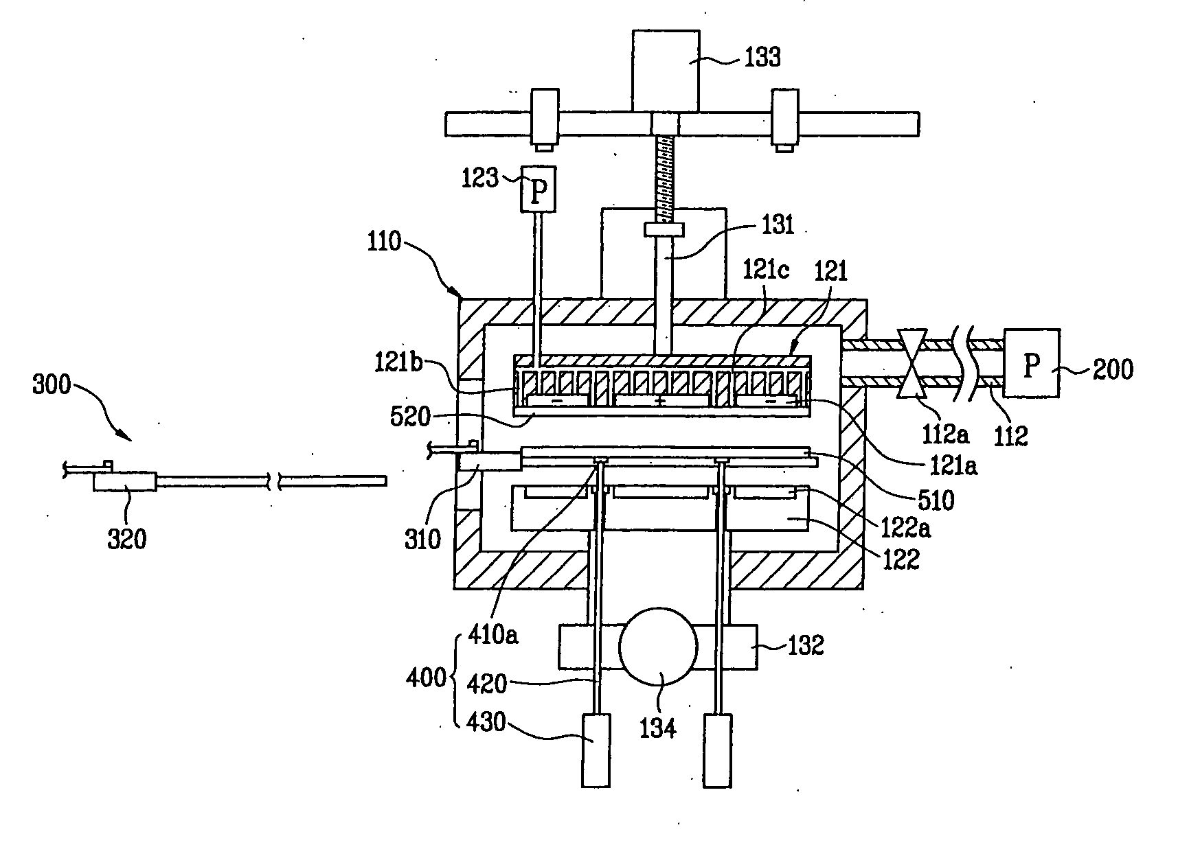
[0037]FIG. 3 is a cross sectional view of an exemplary apparatus including a substrate lifting system according to the present invention. In FIG. 3, the apparatus may include a vacuum processing chamber 110, an upper stage 121, a lower stage 122, an upper stage moving system 131 and 133, a lower stage moving system 132 and 134, a vacuum device 200, a loader part 300, and a first substrate lifting system 400.

[0038] The vacuum processing chamber 110 may include an air outlet 112 transferring a vacuum force to decrease a pressure at an interior of the vacuum processing chamber 110. The upper and lower stages 121 and 122 may be provided at upper and lower spaces at an interior of the vacuum processing chamber 110, respectively. In addition, the upper and lower stages 121 and 122 receive first and second substrates 510 and 520...


PUM

PropertyMeasurementUnit
areaaaaaaaaaaa
electrically conductiveaaaaaaaaaa
vacuum forceaaaaaaaaaa

Abstract

An apparatus for manufacturing a liquid crystal display device includes a unitary vacuum processing chamber, upper and lower stages confronting each other at upper and lower spaces inside the vacuum processing chamber to bond a first and second substrates, and a first substrate lifting system formed in the lower stage for lifting the second substrate.

Description

[0001] The present invention claims the benefit of Korean Patent Application No. P2002-9614 filed in Korea on Feb. 22, 2002, which is hereby incorporated by reference. BACKGROUND OF THE INVENTION [0002] 1. Field of the Invention [0003] The present invention relates to a manufacturing apparatus, and more particularly, to an apparatus for manufacturing a liquid crystal display suitable for a large-sized liquid crystal display. [0004] 2. Discussion of the Related Art [0005] In general, recent developments in the information communication field have increased demand for various types of displays devices. In response to this demand, various flat panel type displays such as liquid crystal display (LCD), plasma display panel (PDP), electro-luminescent display (ELD), and vacuum fluorescent display (VFD) have been developed to replace conventional cathode ray tube (CRT) devices. In particular, LCD devices have been used because of their high resolution, light weight, thin profile, and low po...

Claims


Application Information

Patent Timeline
Patent Type & Authority Applications(United States)
IPC IPC(8): G02F1/13G02F1/1333H01L21/00H01L21/677H01L21/683H01L21/687
CPCH01L21/67092H01L21/68778H01L21/68742H01L21/67748G02F1/13
Inventor LEE, SANG SEOKPARK, SANG HO
Owner AVACO
Why Eureka
Try Eureka