Power semiconductor module and method for producing it

a technology of power semiconductor modules and semiconductor components, applied in semiconductor devices, semiconductor/solid-state device details, electrical apparatuses, etc., can solve the problems of complex and expensive adjustment of flexible printed circuit boards to power semiconductor components, inability to have compact structures, and other contact faces, etc., to achieve reliably and extremely compact design, low number of individual steps

a technology of power semiconductor modules and semiconductor components, applied in semiconductor devices, semiconductor/solid-state device details, electrical apparatuses, etc., can solve the problems of complex and expensive adjustment of flexible printed circuit boards to power semiconductor components, inability to have compact structures, and other contact faces, etc., to achieve reliably and extremely compact design, low number of individual steps

US20050127503A1Inactive Publication Date: 2005-06-16SEMIKRON ELECTRONICS GMBH & CO KG

Image

  • Power semiconductor module and method for producing it
  • Power semiconductor module and method for producing it
  • Power semiconductor module and method for producing it

Examples


Embodiment Construction

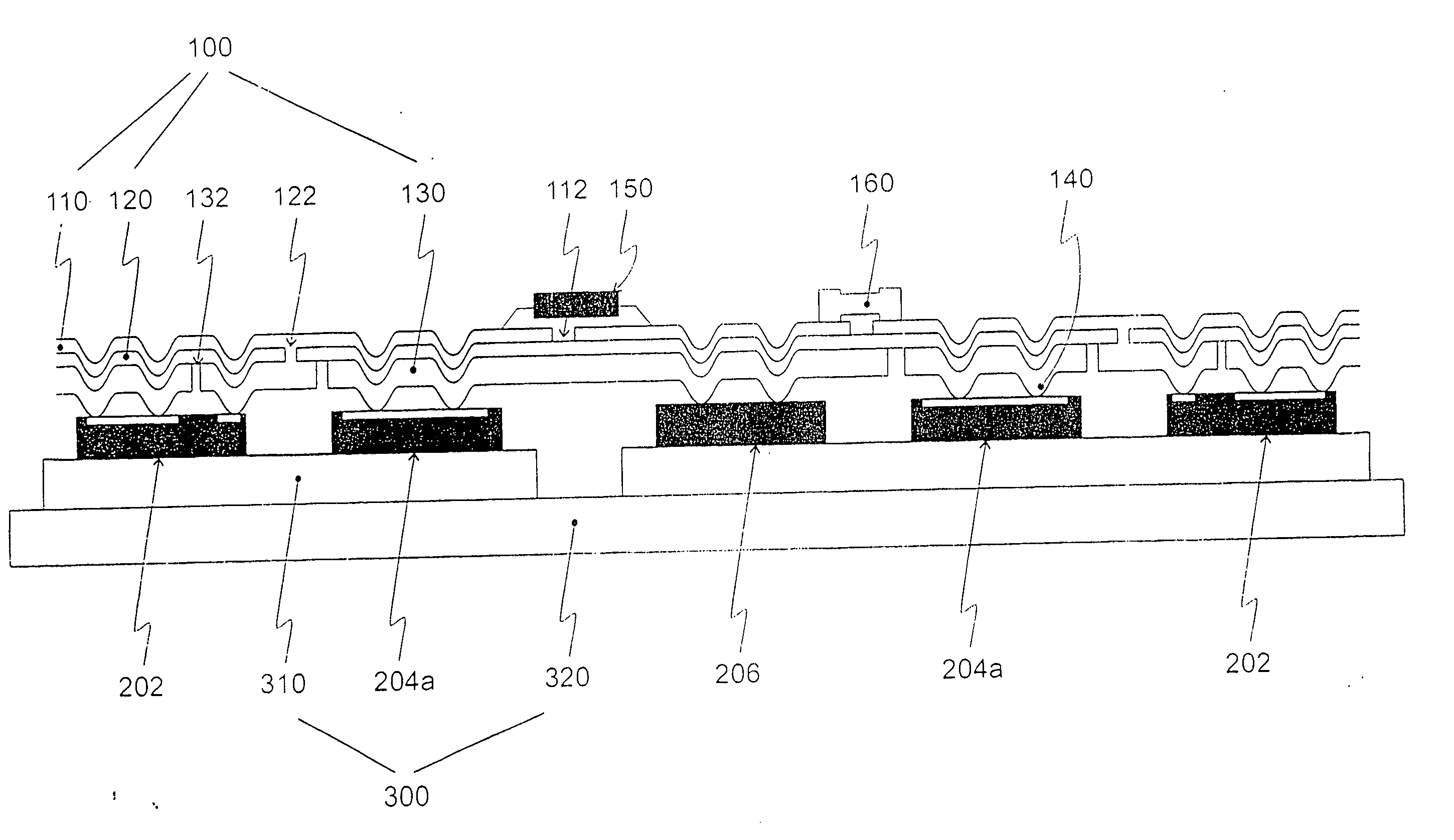
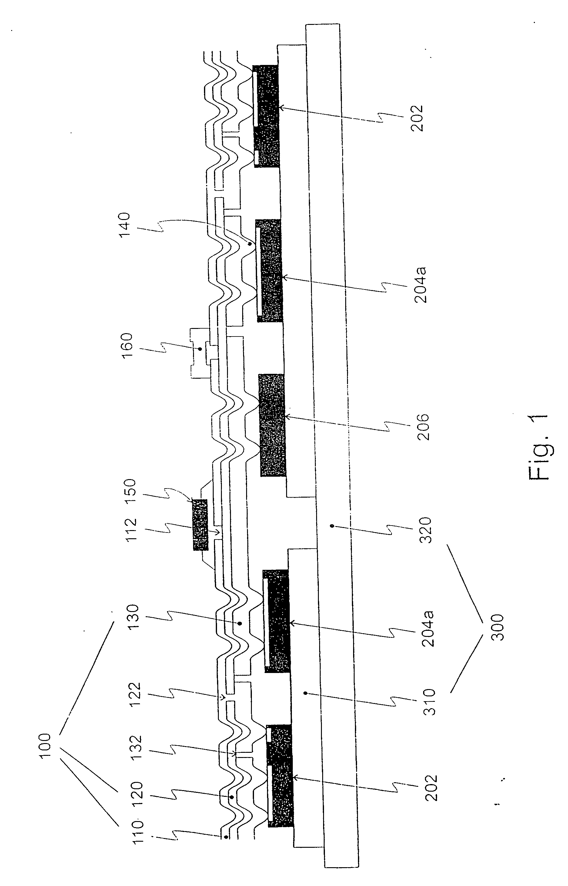
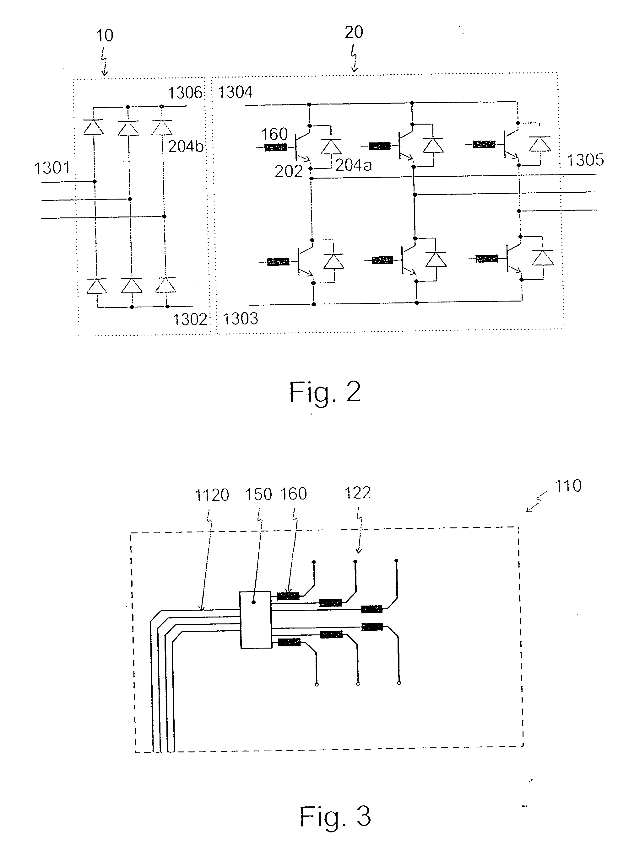
[0027]FIG. 1 shows an embodiment of a power semiconductor module of the invention in a sectional view taken along the line A-A of FIGS. 4 and 5. This power semiconductor module comprises a substrate 300, which in turn comprises an insulating body 320 and conductor tracks 310 that are disposed on insulating body 320 and structured to suit the circuitry with which the module is used. A composite of power semiconductor components 202, 204, spacer elements 206, and a foil composite 100 is disposed on conductor tracks 310. To that end, composite 100 is soldered to conductor tracks 310. Known alternatives to this procedure are adhesive bonds or a plated-through hole.

[0028] The composite of power semiconductor components 202, 204, spacer elements 206 and foil composite 100 is in turn created by means of an ultrasonic welded connection of stamped contact humps 140 of foil composite 100 to spacer elements 206 and power semiconductor components 202, 204.

[0029] Foil composite 100 itself comp...


PUM


Abstract

A power semiconductor module and a method for producing it, wherein the module includes a substrate, with conductor tracks disposed on it to suit circuitry with which the module is used and with power semiconductor components disposed on the conductor tracks. Also disposed on the conductor tracks are spacer elements and a foil composite that includes two metal foil layers with an electrically insulating foil layer disposed between them. The foil composite has contact humps and plated-through holes. At least one of the metal foil layers is structured in a manner to suit the circuitry with which the module is used, and this foil composite is durably connected to the power semiconductor components and to the spacer elements, preferably by ultrasonic welding.

Description

BACKGROUND OF THE INVENTION [0001] 1. Field of the Invention [0002] The invention is directed to a power semiconductor module and a method for producing a power semiconductor module, and more particularly, to a method and apparatus for connecting semiconductor components, especially power semiconductor components such as transistors, thyristors or diodes, with one another and / or with associated supply leads. [0003] 2. Description of the Related Art [0004] Such power semiconductor modules are the subject of constant research, directed toward increasing their performance and reliability, lengthening their service life, and simultaneously reducing their production cost and size. [0005] The points of departure for the invention are the following German Patent Applications of the assignee of the present application: DE 101 21 970 A1, and DE 102 58 565, the latter not having been published by the priority date of the present application. DE 101 21 970 discloses a power semiconductor modul...

Claims


Application Information

Patent Timeline
16 Jun 2005
Publication
US20050127503A1
IPC
H01L21/60; H01L25/00; H01L21/607; H01L23/538; H01L25/07; H01L25/18
CPC
H01L23/5385; H01L23/5387; H01L2924/1301; H01L23/5389; H01L24/24; H01L24/28; H01L24/29; H01L24/72
Inventors
GOBL, CHRISTIAN; HEILBRONNER, HEINRICH