Power amplifier (PA) efficiency with low current DC to DC converter

a technology of power amplifier and converter, which is applied in the direction of amplifiers, amplifiers with semiconductor devices only, amplifiers with semiconductor devices, etc., can solve the problems of high cost and size, the size and conversion efficiency of this regulator type is more problematic, and the complexity of the power supply

Active Publication Date: 2005-12-29
SKYWORKS SOLUTIONS INC
View PDF9 Cites 34 Cited by
  • Summary
  • Abstract
  • Description
  • Claims
  • Application Information

AI Technical Summary

Benefits of technology

[0008] In accordance with the invention there is provided a power amplifier (PA) circuit comprising: a PA output stage having a first amplifying portion having a first amplification and disposed in parallel with a second amplifying portion having a second amplification portion, the PA output stage having an output stage input port for receiving of a RF input signal, an output stage output port for providing of an amplified RF signal, and an output stage amplification being the amplification from the output stage input port to the output stage output port; at least a biasing circuit for biasing of at least one of the first amplifying portion and the second amplifying portion; a DC to DC converter circuit coupled with the second amplifying portion for providing of a second converted output voltage to the second amplifying portion; a first control port coupled with the DC to DC converter and for receiving a first control signal to control the DC to DC converter second converted output voltage in dependence upon a predetermined signal strength of the amplified RF signal at the output stage output port; and, a second control port coupled with the at least a biasing circuit and for receiving a second control signal to control the at least a biasing circuit in such a manner that a ratio of RF input signal amplification between the first amplification and the second amplification varies in dependence upon the predetermined signal strength at the output stage output port.
[0009] In accordance with the invention there is provided a method of controlling PA linearity and power consumption comprising: providing of a PA output stage having a first amplifying portion having a first amplification and a second amplifying portion having a second amplification that is greater than the first amplification, where the first amplification and the second amplification together form an output stage amplification; providing of a DC to DC converted for providing a converted output voltage; receiving of a RF input signal by the PA output stage; determining whether a signal power of the RF input signal is one of below a threshold signal power level and above the threshold signal power level; when the signal power of the RF input signal is below the threshold signal power level: biasing of the first amplifying portion with a low bias voltage; when the signal power of the RF input signal is above the threshold signal power level: biasing of the first amplifying portion with a high bias voltage that is higher than the low bias voltage; biasing of the second amplifying portion using the converted output voltage received from the DC to DC converter; and, amplifying of the RF input signal to form a RF output signal that is an amplified version of the RF input signal.
[0010] In accordance with the invention there is provided a power amplifier (PA) comprising: a PA output stage having a first amplifying portion having a first amplification and disposed in parallel with a second amplifying portion having a second amplification, the PA output stage having an output stage input port for receiving of a RF input signal, an output stage output port for providing of an amplified RF signal, and an output stage amplification being the amplification of the RF input signal from the output stage input port to the output stage output port; a DC to DC converter circuit comprising a first control port for receiving a first control signal for controlling the DC to DC converter for providing of a second converted output voltage to the second amplifying portion in dependence upon a predetermined signal strength of the amplified RF signal at the output stage output port; and, at least a biasing circuit for biasing the first amplifying portion in dependence upon the first control signal for amplifying the RF input signal such that for the output stage amplification a ratio between the first amplification and the second amplification varies in dependence upon the first control signal.

Problems solved by technology

Unfortunately, envelope tracking requires a complex power supply and has yet to be demonstrated in a practical fashion.
Unfortunately, the standard approach in using a DC to DC converter requires very large regulator components capable of delivering an output signal current of over 700 mA with a clean output spectrum.
In general, the size and conversion efficiency of this regulator type is more problematic at high current due to dropping losses in pass transistors.
Thus, using prior art DC to DC converter technology result in high cost and size issues.
Additionally, the challenge in using the prior art circuits arises when these circuits are used in current sensitive devices, such as portable electronic devices.

Method used


Image

  • Power amplifier (PA) efficiency with low current DC to DC converter
  • Power amplifier (PA) efficiency with low current DC to DC converter
  • Power amplifier (PA) efficiency with low current DC to DC converter

Examples


first embodiment

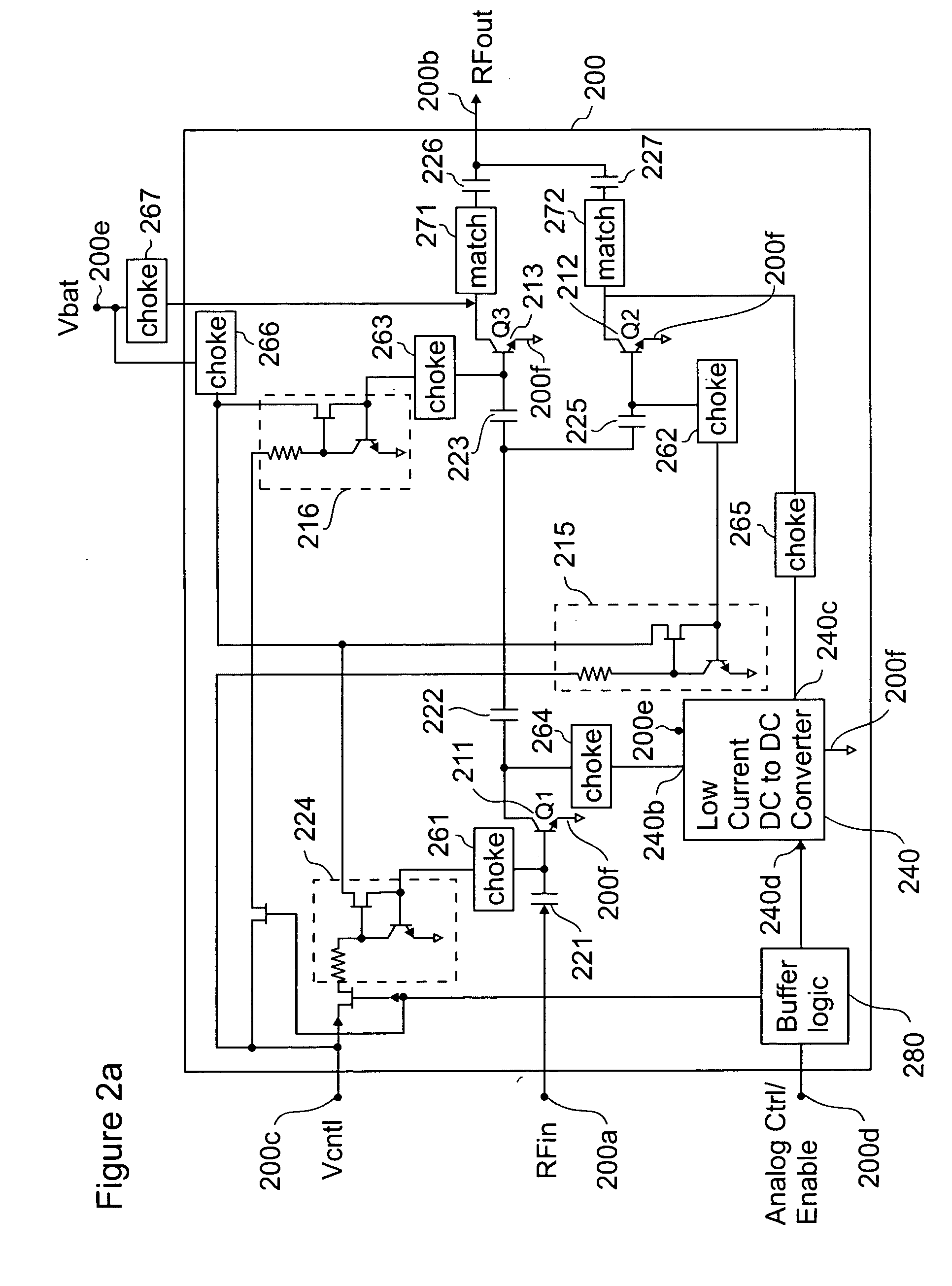
[0023]FIG. 2a illustrates a two-stage power amplifier integrated circuit (PAIC) 200, which includes a low current DC to DC converter 240, which is integrated as part of the PAIC 200, and analog bias control, in accordance with the invention. An input stage of the two-stage amplifier circuit is comprised of a first transistor (Q1) 211. An output amplification stage of the two-stage, or multi-stage, amplifier having an output stage amplification is comprised of a first amplifying portion having a first amplification and including a third transistor (Q3) 213 and a second amplifying portion having a second amplification and including a second transistor Q2212. The first amplification and the second amplification together form the output stage amplification.

[0024] Transistors Q1211 and Q3213 are capacitively coupled to each other using capacitors 222 and 223 disposed in series between the collector terminal of Q1211 and the base terminal of Q3213. The base terminal of transistor Q2212 is...

second embodiment

[0035]FIG. 3 illustrates a two-stage power amplifier integrated circuit (PAIC) 300, which includes a low current DC-to-DC converter 340 and an automatic bias control circuit 350, in accordance with the invention. An input stage of the two-stage amplifier circuit is comprised of a first transistor Q1311. An output amplification stage of the PAIC 300 having an output stage amplification is comprised of a first amplifying portion having a first amplification and including a third transistor Q3313 and a second amplifying portion having a second amplification and including a second transistor Q2312. The first amplification and the second amplification together form the output stage amplification.

[0036] A RF input port 300a of the PAIC 300 is coupled using a capacitor to a first RF power detector 351, which is further capacitively coupled using capacitor 321 to the base terminal of transistor Q1311. The collector terminal of transistor Q1311 is coupled to a coupling capacitor 322, which i...


PUM


Abstract

A novel method and apparatus is disclosed for reducing power dissipation of RF power amplifiers when a reduced output power level is required. The mechanism has the specific purpose of optimizing the collector terminal voltage on portions of the amplifier's RF chain for maintaining linearity while minimizing power consumption. The apparatus permits a smaller DC to DC converter to be used than in prior art, such that it is implemented in the same semiconductor die or module. Furthermore, the invention eliminates the amplification and phase continuity issues that arise from switched state power amplifiers and envelope-following approaches.

Description

FIELD OF THE INVENTION [0001] The invention relates to the field of low current power amplifier consumption and more specifically to the field of low current power amplifier consumption by using a DC to DC voltage conversion circuit. BACKGROUND OF THE INVENTION [0002] Many people desire a longer operating lifetime for their battery-powered electronic, such as mobile telephones, MP3 players, and so forth. Typically in order for these battery-powered devices to conserve electrical power, their current consumption is managed preferably retaining operating characteristics thereof unaltered over as much of the battery operating range as possible. [0003] Numerous techniques and publications exist, which detail methods and apparatus for improving power amplifier (PA) power consumption by varying supply voltage provided thereto using a DC to DC converter. For example, U.S. Pat. No. 6,624,702, discloses circuitry for controlling of a DC to DC converter in dependence upon sensed RF output sig...

Claims


Application Information

Patent Timeline
Patent Type & Authority Applications(United States)
IPC IPC(8): H03F1/02H03F1/06H03F3/04H03F3/191H03F3/21
CPCH03F1/02H03F1/0205H03F3/21H03F3/191H03F1/0227
Inventor DOHERTY, MARKQUAGLIETTA, ANTHONYHARRISON, JOSE
Owner SKYWORKS SOLUTIONS INC
Why Eureka
Try Eureka