

Semiconductor device
a technology of semiconductor devices and films, applied in semiconductor devices, semiconductor/solid-state device details, radiation control devices, etc., can solve the problems of not being able to form whole dummy vias, not being able to place the dummy via that connects interconnects respectively formed, and having different electric potentials, so as to improve the adhesiveness of films, and increase the effect of an additional process
- Summary
- Abstract
- Description
- Claims
- Application Information
AI Technical Summary
Benefits of technology
Problems solved by technology
Method used
Image

Examples
example
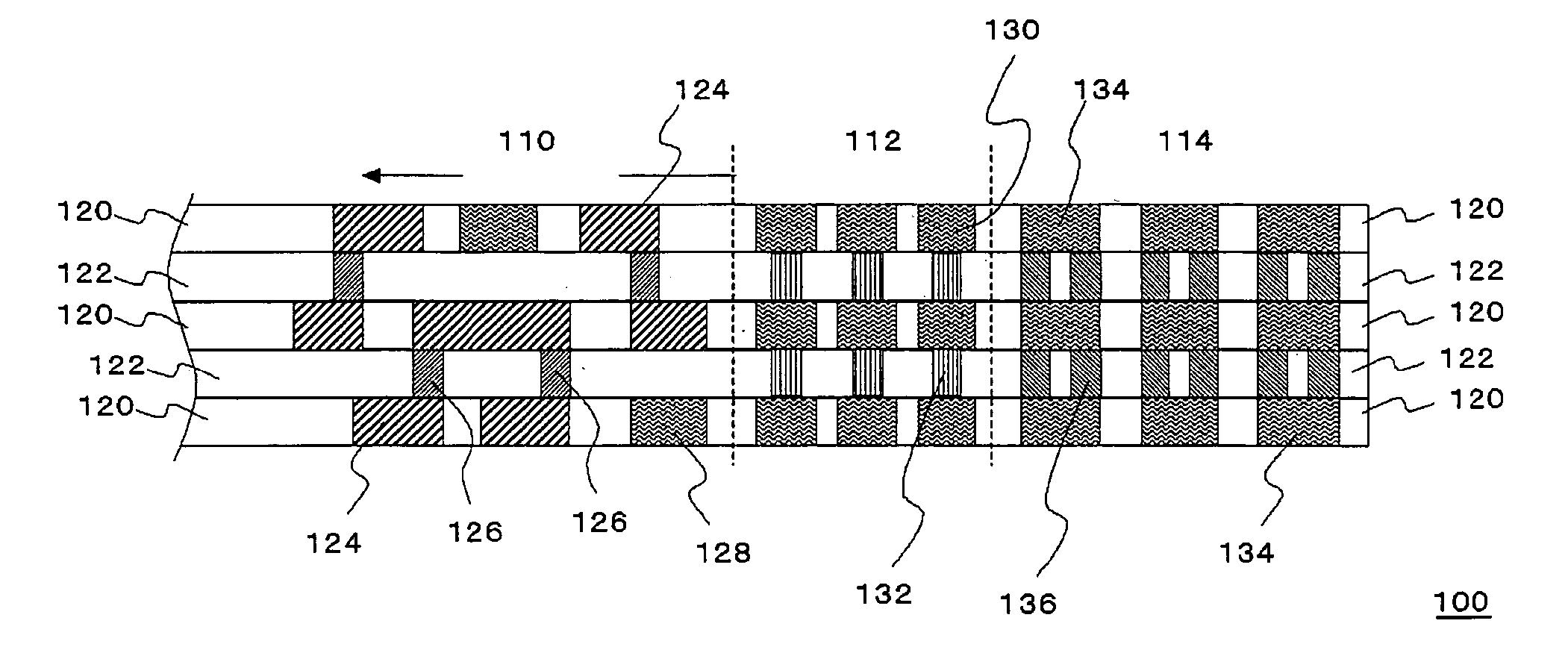
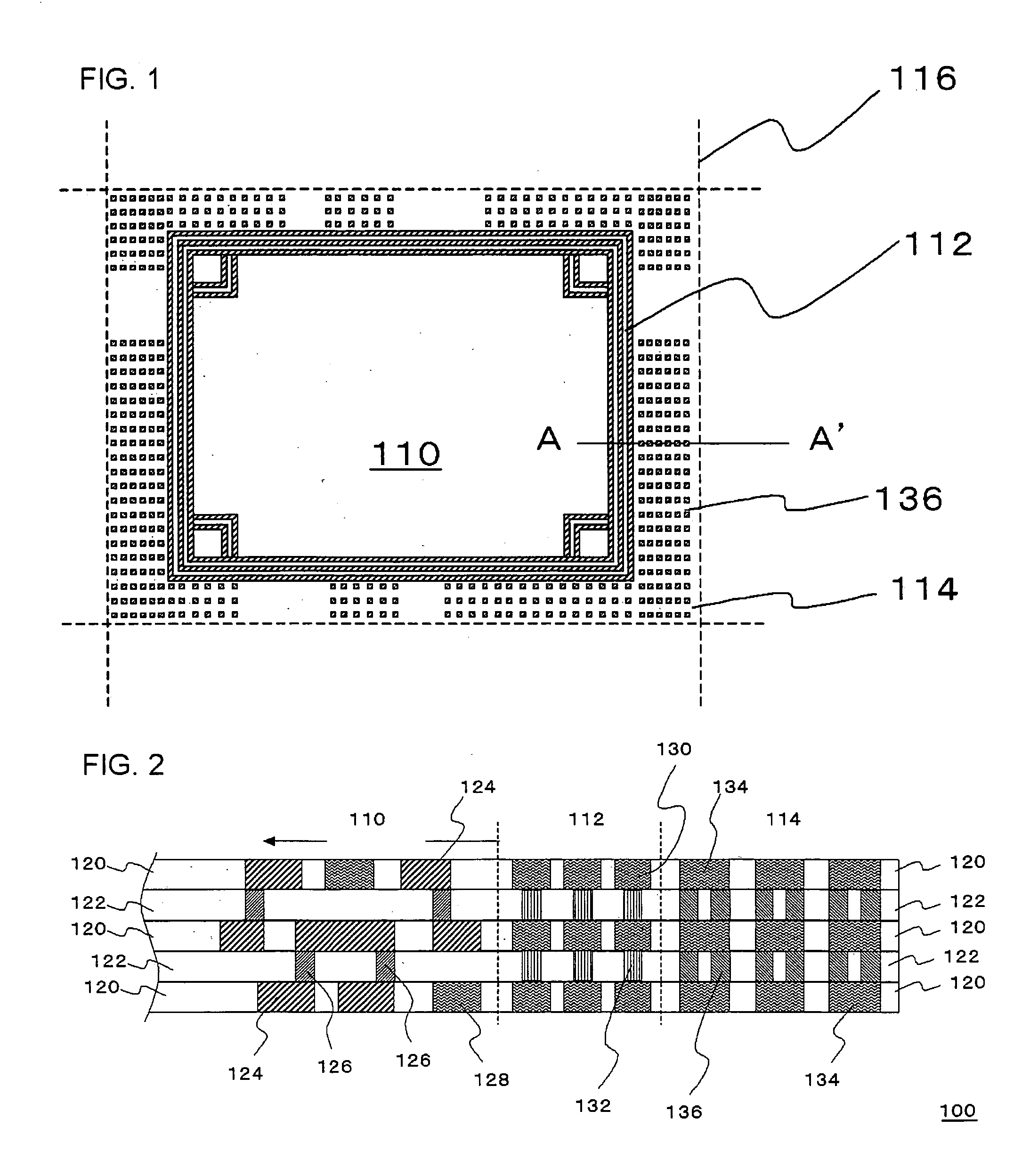
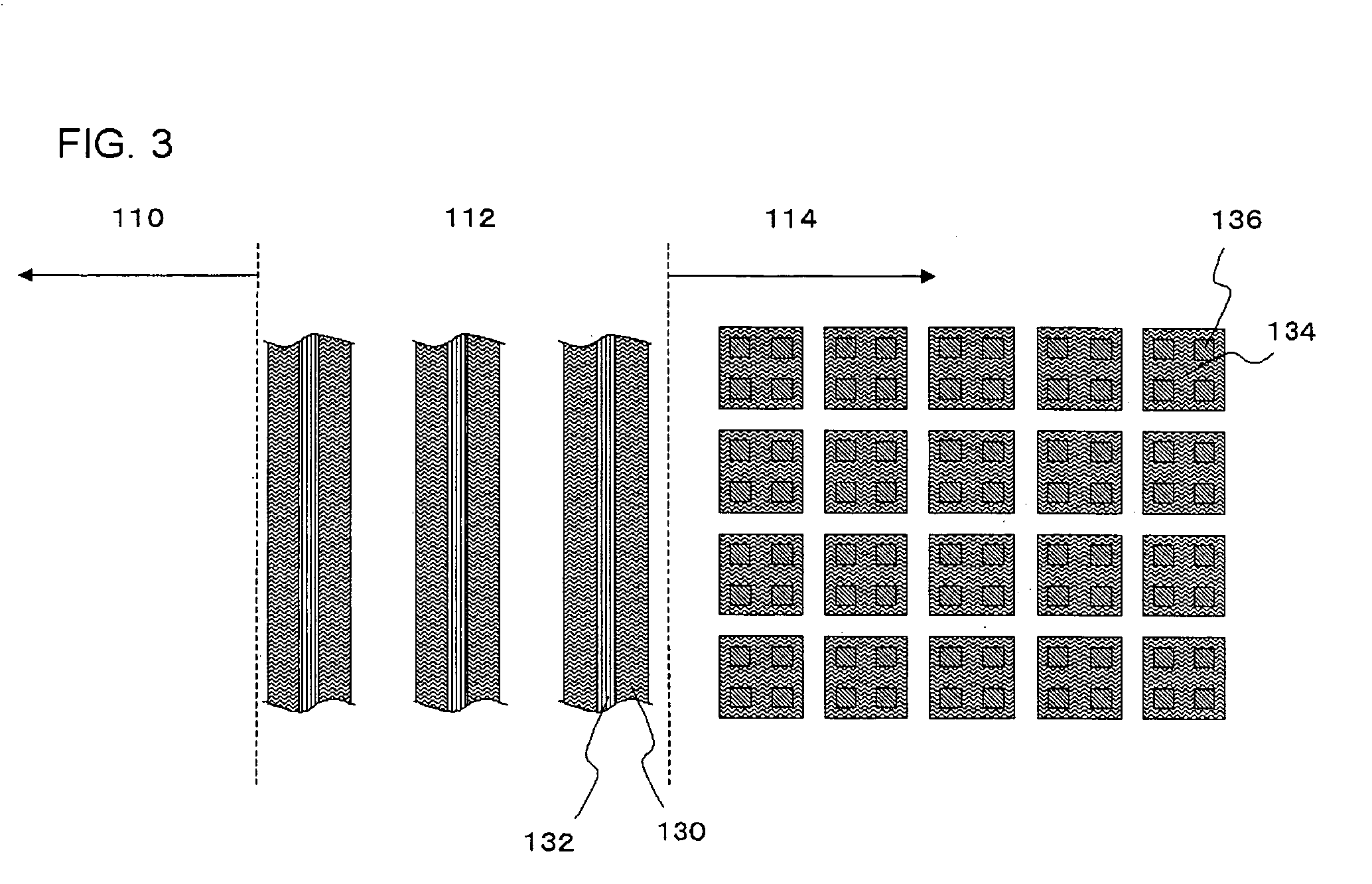
[0061] A semiconductor chip, size of which is 20 mm×20 mm, having a multilayer wiring structure of nine layers and copper interconnects in which low-dielectric-constant insulating films (SiOC) having the relative dielectric constant of 2.3 are used as the interlayer dielectric film was obtained. In the semiconductor chip, the dummy vias were provided at the peripheral region thereof where the content rate of metals in the region was 11%. At the same time, a reference semiconductor chip having the same structure as described above but no dummy vias were provided was obtained.
[0062] To each of the semiconductor chips, heat cycles from −60 to 150 degree centigrade were applied for a thousand (1,000) times. As a result, almost no peeling-off of the films was seen on the semiconductor chip with the dummy vias. On the contrary, as for the reference semiconductor chip without the dummy vias, peeling-off of the films was seen to the extent of no less than 80%.
[0063] While the preferred em...
PUM
 Abstract
Description
Claims
Application Information