Electronic circuit, electronic device, method of driving electronic device, electro-optical device, and electronic apparatus

a technology of electronic devices and circuits, applied in static indicating devices, instruments, photoelectric discharge tubes, etc., can solve the problems of reducing the total number of transistors in each unit circuit, increasing manufacturing costs, and difficulty in ensuring the time-emitting period

Inactive Publication Date: 2007-02-22
SEIKO EPSON CORP
View PDF13 Cites 7 Cited by
  • Summary
  • Abstract
  • Description
  • Claims
  • Application Information

AI Technical Summary

Benefits of technology

[0011] According to this aspect, a data signal is supplied to the input terminal of the driving unit from the second wiring line through the switching element in a first period. If the reference signal varies after the first period passes, by the capacitive coupling in the capacitor element, the potential of the input terminal varies from the potential of the data signal in the first period by the variation in the reference signal. Accordingly, the driven element that is supplied with the driving voltage or the driving current in a driving period having a time length according to the potential of the input terminal is driven in a state according to the data signal. In addition, since the potential of the second electrode of the capacitor element is directly set by the reference signal line, it is possible to set the potentials at the two electrodes of the capacitor element in a short time.
[0030] According to this aspect, the data signal is held in the second electrode in the first period, and the voltage of the second electrode temporally varies in the second period. In addition, the voltage of the first electrode (that is, voltage of the gate of the driving transistor) varies by the voltage value according to the difference between the levels of the data signal and the control signal through the capacitive coupling in the capacitor element. Accordingly, according to this aspect, it is possible to drive the driven element over the time length according to the data signal. Further, if the configuration in which the first electrode enters a floating state in the second period is adopted, it is possible to suppress the charge accumulated in the first electrode from leaking. Therefore, it is possible to set the voltage of the first electrode to the voltage according to the data signal in high precision.

Problems solved by technology

If the total number of transistors is large, a structure of a unit circuit becomes complicated, which results in increasing the manufacturing cost.
However, according to the related art, there is a limit in that the total number of transistors in each unit circuit is reduced.
As such, in a structure in which the scanning period and the light-emitting period are individually set in one frame, it is difficult to sufficiently ensure the time length of the light-emitting period.
In addition, if the time length of the light-emitting period is insufficient, the luminance of each OLED element may be insufficient, and thus display becomes darker.
However, in an electro-optical element, such as an OLED element or the like, a current may be concentrated in a short period (for example, a spike current may be supplied), and thus characteristic deterioration may occur.
Meanwhile, in the first terminal of the driving transistor, the voltage value may accidentally vary due to the external disturbance, such as noise.

Method used


Image

  • Electronic circuit, electronic device, method of driving electronic device, electro-optical device, and electronic apparatus
  • Electronic circuit, electronic device, method of driving electronic device, electro-optical device, and electronic apparatus
  • Electronic circuit, electronic device, method of driving electronic device, electro-optical device, and electronic apparatus

Examples


first embodiment

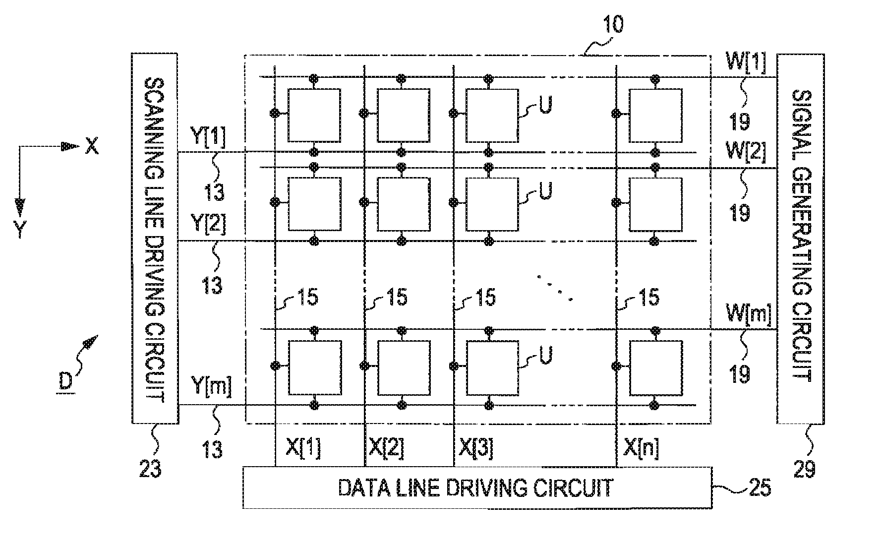
[0072]FIG. 1 is a block diagram illustrating a structure of an electronic device according to a first embodiment, of the invention. An electronic device D shown in FIG. 1 is corresponds to an electro-optical device that is used in various electronic apparatuses as an image display device, and includes an element array unit 10 in which a plurality of unit circuits U are two-dimensionally disposed, and various circuits a scanning line driving circuit 23, a data ling driving circuit 25, and a signal generating circuit 27) that drives the unit circuits U. In this case, each of the scanning line driving circuit 23, the data line driving circuit 25, and the signal generating circuit 27 may be mounted on the electronic device D as an independent circuit, or a portion or all of these circuits may be mounted on the electronic device D as a single circuit.

[0073] As shown in FIG. 1, the element array unit 10 includes m scanning lines 13 that extend in an X direction, m reference signal lines ...

second embodiment

[0093] Next, a second embodiment of the invention will be described. In the second embodiment, the same constituent elements as the first embodiment are denoted by the same reference numerals, and the description thereof will be appropriately omitted.

[0094]FIG. 5 is a circuit diagram illustrating a structure of one unit circuit U in an electronic device D according to the present embodiment. As shown in FIG. 5, the unit circuit U according to the present embodiment has a structure in which an n-channel-type transistor 37 is additionally provided in the structure according to the first embodiment shown in FIG. 3. The transistor 37 corresponds to a switching element that is interposed between the input terminal T and the output terminal of the inverter 34 and controls electrical connection between the input terminal T and the output terminal of the inverter 34 (conduction or non-conduction).

[0095] The gate of the transistor 37 is coupled to a wiring line that is supplied with a rese...

fifth modification

[0105] In the above-mentioned embodiments, the OLED element has been exemplified as the electro-optical element 35. However, the electro-optical element that is adopted in the electronic device of the invention is not limited thereto. For example, in addition to the OLED element, various self-emission elements, such as an inorganic EL element, a field emission (FE) element, a surface-conduction electron-emitter (SE) element, a ballistic electron surface emitting (BS) element, and a light-emitting diode (LED) element, and various electro-optical elements, such as an electrophoresis element, an electrochromic element, or the like, may be used. Further, the invention may be applied to a sensing device, such as a biochip or the like. In the invention, the driven element is a concept that includes all elements driven by applying an electric energy. The electro-optical element such as the light-emitting element is only an example of the driven element.


PUM


Abstract

An electronic device includes a plurality of first wiring lines, a plurality of second wiring lines that intersect the plurality of first wiring lines, a plurality of unit circuits that are disposed so as to correspond to intersections between the plurality of first wiring lines and the plurality of second wiring lines, and a plurality of reference signal lines that supply reference signals to the plurality of unit circuits. Each of the plurality of unit circuits has a driven element that is driven by a driving voltage or a driving current, a driving unit that supplies the driving voltage or the driving current to the driven element, a switching element that controls electrical connection between an input terminal provided in the driving unit and one of the plurality of second wiring lines, and a capacitor element that has a first electrode connected to the input terminal and a second electrode connected to one of the plurality of reference signal lines, and accumulates a charge between the first electrode and the second electrode.

Description

BACKGROUND [0001] 1. Technical Field [0002] The present invention relates to a technology for controlling behaviors or various driven elements, such as an organic light-emitting diode (hereinafter, referred to as ‘OLED’) element, a liquid crystal element, an electrophoresis element, an electrochromic element, an electron emission element, a resistor element, or the like. [0003] 2. Related Art [0004] In general, various technologies for driving driven elements have been suggested. For example, in JP-A-2003-122301 (see FIG. 1), a structure is disclosed in which a plurality of unit circuits having OLED elements that serve as driven elements are two-dimensionally disposed. Each of the unit circuits includes a driving transistor that controls a current supplied to the OLED element according to a gate voltage, a reset transistor that causes the driving transistor to be diode-connected, and a light-emitting control transistor that switches whether the current is supplied to the OLED elemen...

Claims


Application Information

Patent Timeline
Patent Type & Authority Applications(United States)
IPC IPC(8): H01J40/14
CPCH03F2200/303H03F3/08G09G3/30G09G3/20G09G3/32G09G3/36
Inventor MIYAZAWA, TAKASHI
Owner SEIKO EPSON CORP
Why Eureka
Try Eureka