

Compact column redundancy CAM architecture for concurrent read and write operations in multi-segment memory arrays
a memory array and column redundancy cam technology, applied in the field of nonvolatile memory circuits, can solve the problems of significant cost for fabrication and die area, memory cell location faulty, and significant amount of device substrate area dedicated to duplicating registers
- Summary
- Abstract
- Description
- Claims
- Application Information
AI Technical Summary
Problems solved by technology
Method used
Image



Examples
Embodiment Construction
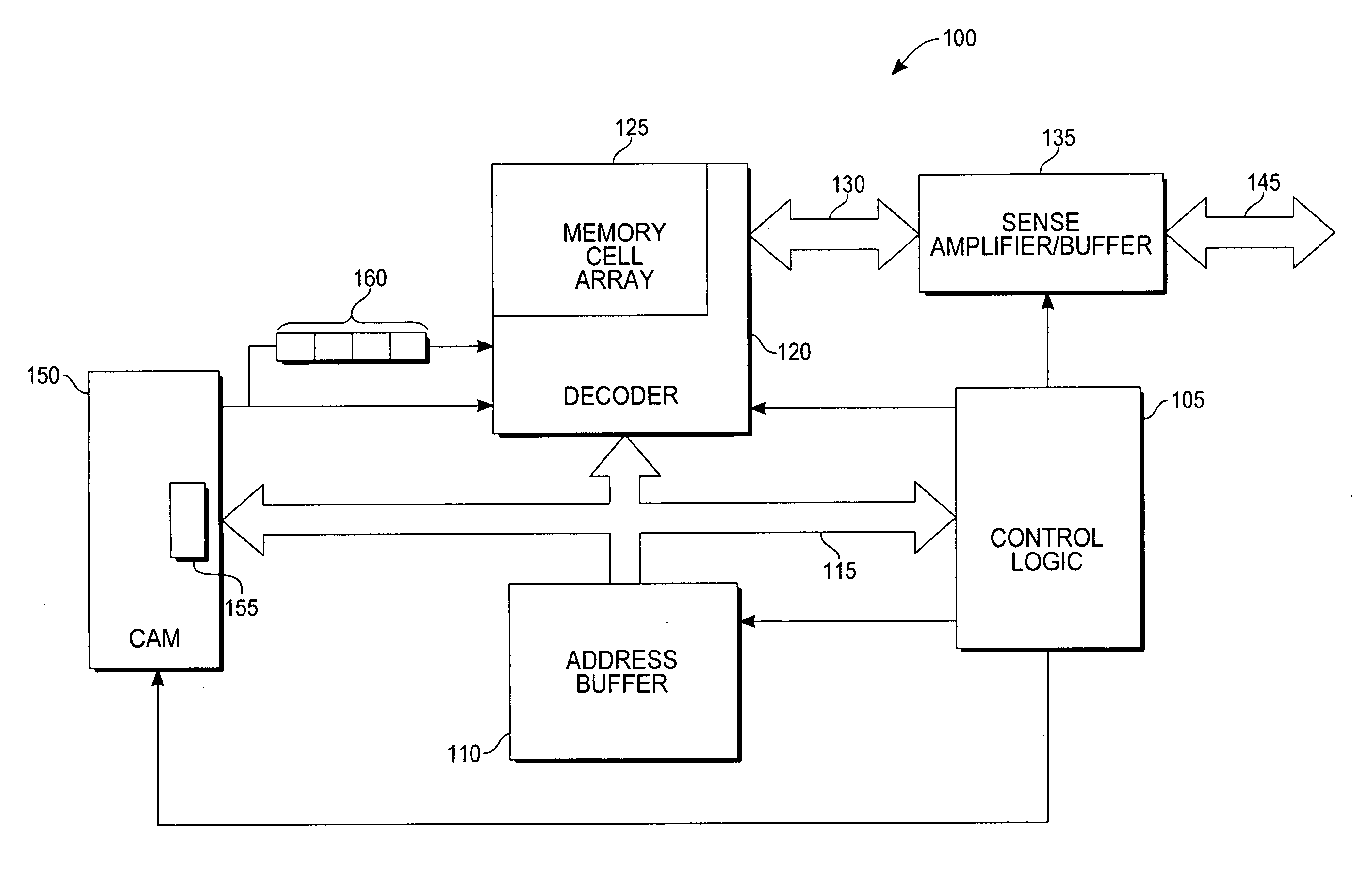
[0012] With reference to FIG. 1, an address buffer 110 receives addresses from a system address bus (not shown) in an exemplary nonvolatile memory system 100. The address buffer 110 communicates with the system address bus and a local address bus 115 under the direction of control logic 105. The control logic 105 also connects to a sense amplifier / buffer 135, a decoder 120 of a memory cell array 125, and a content addressable memory (CAM) 150. The local address bus 115 connects to the control logic 105, the decoder 120, and a memory plane address register 155. The memory plane address register 155 is latched within the CAM 150. A column redundancy register 160 connects between the CAM 150 and the decoder 120. The CAM 150 also connects directly to the decoder 120. A bidirectional memory data bus 130 connects the sense amplifier / buffer 135 with the memory cell array 125. The sense amplifier / buffer 135 connects to a remainder of the external system through a bidirectional data bus 145....
PUM
 Abstract
Description
Claims
Application Information